
Control Circuit
Index 244
The temperature range controller design circuit
Published:2011/6/18 3:03:00 Author:Seven | Keyword: temperature range, design circuit
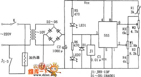
View full Circuit Diagram | Comments | Reading(594)
The color circuit image of the fridge time delay protector
Published:2011/6/19 0:31:00 Author:Seven | Keyword: color circuit image, time delay protector

View full Circuit Diagram | Comments | Reading(529)
The over-voltage auto power-down equipment setting circuit
Published:2011/6/19 0:49:00 Author:Seven | Keyword: over-voltage, power-down
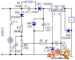
The 220V mains provide with a stable 12V working voltage through C1, VD1 and DW1, and VD3, R2 and RP1 compose a voltage distributing sampling circuit. When the mains voltage is normal, DW2 is blocked, the working voltage on 5-pin of TWH8778 is lower than 1.6V, the relay J is open, the mains provides power normally after crossing the J-1 commonly closed touch spot; when the mains voltage is high than the normal value, DW2 is breakdown and conducting, LEV on 5-pin of TWH8778 is rising to 1.6v, which reverses IC, and the 3-pin outputs a high LEV, the relay is closed and the power supply of the electric apparatus is cut off immediately. (View)
View full Circuit Diagram | Comments | Reading(875)
The NE555 FM modulation circuit
Published:2011/6/19 8:33:00 Author:Seven | Keyword: modulation circuit
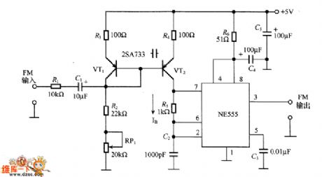
In the figure is the NE555 FM modulation circuit. In the figure, NE555 7-pin is connected with a FM modulation circuit which is composed with R5 and C2, but the frequency range is kind of small. VT1 and VT2 form a current Miller circuit, which generates a charging current in the charging circuit, the current magnitude is decided by R2 and RP1. The low-frequency modulation signal and the bias current IB are added up and then the oscillating frequency is changed. VT1 and VT2 in the current Miller circuit would better be couple pipe.
(View)
View full Circuit Diagram | Comments | Reading(5749)
The FM modulation circuit composed of transistors
Published:2011/6/19 8:48:00 Author:Seven | Keyword: FM modulation circuit, transistors
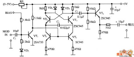
In the circuit, VT2 and VT3 are the multi-resonance oscillator circuit which is coupled by emitters, VT4 and VT5 compose the constant current circuit, which is controlled by the current. By using the clamp diodes of VD2 and VD3 which rise the switch shifting speed, the collecting electrode voltage fluctuation of VT2 and VT3 is kept at 0.5~0.6V. By the figured parameter, when the bias voltage is 5V, the oscillating frequency is f0=3.3×10/C2, and the temperature coefficient is positive to the outside temperature. Because the temperature coefficient of the basic pole-emitting pole voltage UBE of the transistor is passive, then emitting pole current has the positive coefficient.
(View)
View full Circuit Diagram | Comments | Reading(1159)
The variode FM modulation circut
Published:2011/6/19 10:17:00 Author:Seven | Keyword: FM modulation circut
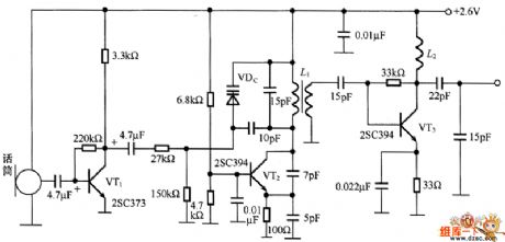
In the circuit, VT1 magnifies the signal generated by the electret capacitance microphone to the value of the VDc working voltage. The LC oscillating circuit, which is composed of VT2 and so on, generates a 80MHz signal. L1 is the oscillating coil with magnetic cores, which can set the value of the oscillating frequency at 76~90MHz. The frequency of the resonance circuit is changed by the variode VDc, and the frequency is FM modulated directly, when the microphone outputs a 3mV current, we can get a ±25kHz MOD. The FM modulation signal is magnified to about 2.3mV by VT3 and then emitted to the sky by the aerial.
(View)
View full Circuit Diagram | Comments | Reading(840)
The IGBT drive circuit composed of discrete components
Published:2011/6/19 10:22:00 Author:Seven | Keyword: drive circuit, discrete components
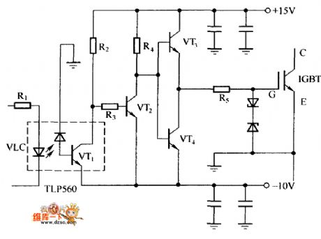
The IGBT drive circuit composed of discrete components
(View)
View full Circuit Diagram | Comments | Reading(4291)
The 7-color circling fancy lamp circuit
Published:2011/6/19 10:25:00 Author:Seven | Keyword: fancy lamp
View full Circuit Diagram | Comments | Reading(708)
The over-voltage circuit of IGBT insulated gate dual-pole transistor grid
Published:2011/6/20 1:14:00 Author:Seven | Keyword: over-voltage, insulated gate, transistor grid
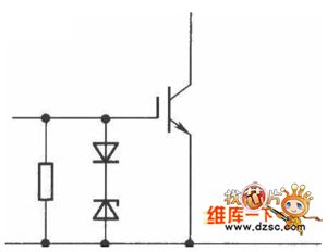
The reason of IGBT grid over-voltage:1. The static electricities assemble at the grid and cause over-voltage; 2. The capacitor Miller effect cause the grid over-voltage.
To prevent IGBT grid-emitter from being over-voltage, we should connect a several KΩ resistor between the grid and emitter of IGBT, see as the figure. The resistor should be close to the grid and the emitter. (View)
View full Circuit Diagram | Comments | Reading(826)
The delayed pulse generating circuit
Published:2011/6/21 2:03:00 Author:Seven | Keyword: delayed pulse, generating
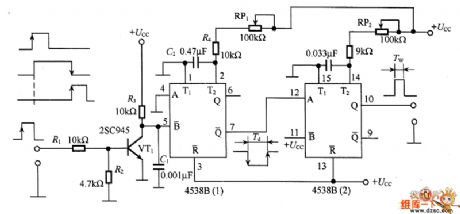
In the figure is the delayed pulse generating circuit, this circuit can recognize the reaction time of the ultrasonic. The spread speed of the sound wave is about 340m/s, if the round-trip of the sound wave is 2~20m, then we need 5.88~58.8ms time delay. If the window detection is done, the window width is 10cm~1m, the trigger pulse width Tw is 300μs~3ms. In the circuit, the delay unit is the CMOS single steady multi-resonance oscillator 4538B. The trigger signal makes the transistor VT1 conducting before it triggers the pulse, when the delay unit begins to time, the pulse width Td=C2(R4+RP1).
(View)
View full Circuit Diagram | Comments | Reading(1289)
The inverting parallel connection or bridge controllable silicon circuit
Published:2011/6/23 19:46:00 Author:Seven | Keyword: parallel connection, controllable silicon circuit
View full Circuit Diagram | Comments | Reading(775)
The high-voltage power supply and lower limit alarm circuit
Published:2011/6/22 1:39:00 Author:Borg | Keyword: high-voltage, power supply, lower limit
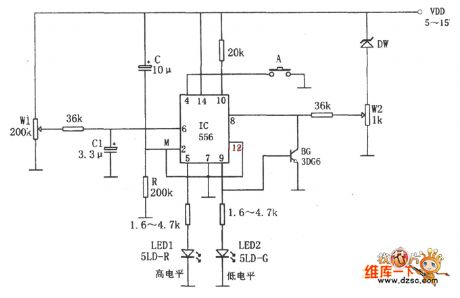
In the circuit is the high-voltage power supply and low limit alarm circuit. The circuit consists of the top limit alarm circuit and the lower limit alarm circuit. The right part is the lower limit alarm circuit: when the power supply voltage is close to the lower limit (but still normal), just adjust the potentiometer Wz, then the LEV of 556 8-pin is a little higher than 1/3VDD. When the power supply moves lower and makes the 8-pin LEV under l/3VDD, the 556 9-pin is reversing and outputting a high LEV, so the lower limit makes LED2 light. At the same time, the transistor BG is connected with 9-pin.
(View)
View full Circuit Diagram | Comments | Reading(872)
The electric whistle alarm circuit
Published:2011/6/23 11:07:00 Author:qqtang | Keyword: electric whistle alarm
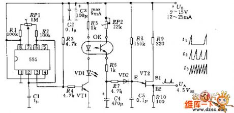
In the figure is the electric whistle alarm circuit that can generate the rising and falling tone sound. The sound is generated by two generators (timer 555 and single knot transistor 2N2648) that are coupled by the photoelectric coupler; The 555 generator produces the 0.3HZ frequency signal, which makes the single knot transistor VT2 sound generator strengthen or weaken in this rhythm.
(View)
View full Circuit Diagram | Comments | Reading(940)
The 555 auto dark room exposure circuit
Published:2011/6/23 4:02:00 Author:qqtang | Keyword: dark room, exposure
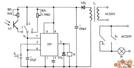
In the figure is the 555 auto dark room exposure circuit. The switch S is the timing gear, when pressing S1, the 3-pin of 555 is outputting a high LEV, the relay K is conducting, the touch spot K1 is closed, lamp h is lighting and exposing, and it is put out in certain. Press S1 again, the exposure will be done again, RP2 is used to adjust the exposure time, which is from 1s to 1min. After the switch S2 is connected with 1, it is working with phototransistor VT and the exposure is done automatically, when it is connected with S, it becomes focusing, and becomes timing by being connected with 3. When S3 is connected, it's manual mode.
(View)
View full Circuit Diagram | Comments | Reading(1203)
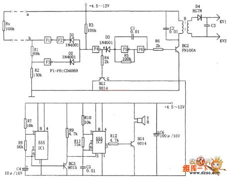
The broken and short multi-line stereo alarm circuit
Published:2011/6/22 3:54:00 Author:Borg | Keyword: multi-line, alarm circuit
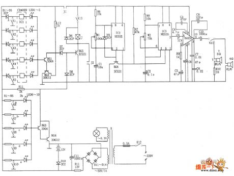
In the figure is the broken and short multi-line stereo alarm circuit. The alarm consists of the rectifier power supply, stereo part, 5 short lines and 5 broken lines of alarm and control circuits. The rectifier power supply consists of D11~D14,R11,C11,D10 and so on, the stereo alarm circuit consists of IC2(NE555) and IC3(NE555), etc. IC4(BA532) is the power amplifier circuit, whose output power can reach 5W. The short or touch alarm part consists of 6-phase inverter IC1(CD4069), BG1, BG2 and so on, when the human body touches either terminal of A~E, as the input terminal of the OR gate is in a low LEV.
(View)
View full Circuit Diagram | Comments | Reading(757)
The XTR110 disorder and span adjusting circuit
Published:2011/6/22 2:37:00 Author:Borg | Keyword: disorder, span adjusting
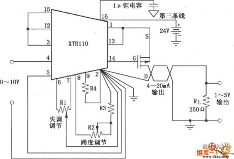
In the figure is the malfunction and span adjusting circuit of 0~10v input voltage and 4~20mA output current. R1 is the disorder adjusting potentiometer, R2 is the span adjusting potentiometer.
Disorder adjusting method: input a low voltage that is not 0, adjust R1 and make the output have a right current value, and then make the input be 0, so that the output must be 0. Span adjusting method: the set input voltage as full scale +10v, adjust R2 to make the current reach to top limit of 20mA. What need to be noticed is that the span adjustment will affect the disorder adjustment. (View)
View full Circuit Diagram | Comments | Reading(1079)
The 8-line digital display superior alarm circuit
Published:2011/6/22 3:08:00 Author:Borg | Keyword: 8-line, display, alarm circuit
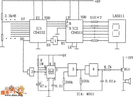
In the figure is the 8-line digital display superior alarm circuit. This circuit consists of the timed stereo circuit, 8-line encoder, decoder, digital display circuit and so on. IC1(CD4532) is the octal prior encoder, and the 8-line input control wires are connected with K0~K7 eight switches, when the input control wire is cut off due to some condition, then input a corresponding high LEV, the encoder will program a 3-bit binary address code. If there are more than 2 lines of wires cut off, the encoder will react to the line of the superior stage.
(View)
View full Circuit Diagram | Comments | Reading(1582)
The high voltage code protection alarm circuit
Published:2011/6/22 1:57:00 Author:Borg | Keyword: high voltage, protection
In the circuit is the high voltage code protection alarm circuit. The alarm uses resistance code to recognize the true or false, so it can be used to the door, window, handbag, lock case and so on. The core of the circuit is the multi-resonance oscillating stereo circuit, the chip CD4069 and transformer B are used as the drive stage. In the circuit, when a and b is broken down or short, the resistance of the resistor Rx may rise or fall, which leads to the high output LEV of F4 OR gate circuit(e point), so the pipe BG1 is conducting, and the stereo circuit is passable, which generates the dual sound alarm signals.
(View)
View full Circuit Diagram | Comments | Reading(753)
AC power control photocell memory switch circuit
Published:2011/6/22 3:20:00 Author:TaoXi | Keyword: AC, power control, photocell, memory switch

We can use the flash beam to supply the remote control for the AC power devices. The important point of this device is the memory function. It can continuously supply the power to the device. When it acts the second time, the power will be cut off continuously. It is composed of a high sensitivity photocell, a high-gain integrated circuit Schmitt trigger and a pulse-driven locking relay.
(View)
View full Circuit Diagram | Comments | Reading(2926)
Servo motor speed control circuit
Published:2011/6/22 19:15:00 Author:TaoXi | Keyword: Servo motor, speed, control circuit
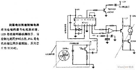
The servo motor speed control circuit connects the photoelectric encoder with the motor shaft, the LED is the indicator light of the PLL detection, it turns on when the control circuit is synchronous. The PLL is the phase synchronous control method of the electrical moter, it uses the chip of TC9142.
(View)
View full Circuit Diagram | Comments | Reading(4600)
| Pages:244/312 At 20241242243244245246247248249250251252253254255256257258259260Under 20 |
Circuit Categories
power supply circuit
Amplifier Circuit
Basic Circuit
LED and Light Circuit
Sensor Circuit
Signal Processing
Electrical Equipment Circuit
Control Circuit
Remote Control Circuit
A/D-D/A Converter Circuit
Audio Circuit
Measuring and Test Circuit
Communication Circuit
Computer-Related Circuit
555 Circuit
Automotive Circuit
Repairing Circuit