
Control Circuit
Index 253
MAX038 inside casing circuit
Published:2011/6/8 8:02:00 Author:chopper | Keyword: inside casing
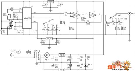
Frequency in every frequency band is controlled by RP1 and RP2.RP1 is coarse adjustable potentiometer.The charge current of oscillating capacitor CF is changed by altering the value of RP1 in order tochange the frequency.RP2 is fine tuning potentiometer,and it changes output frequency by changing the value of UFADJ.The variation range of RP2 is not great,and it is usedas a vernier regulation.The dutyfactor of every waveform is fixed as 50% so that can simplify the circuit.This has been able to satisfy many occasions. (View)
View full Circuit Diagram | Comments | Reading(3227)
max038 function signal generator circuit
Published:2011/6/8 7:50:00 Author:chopper | Keyword: function, signal generator
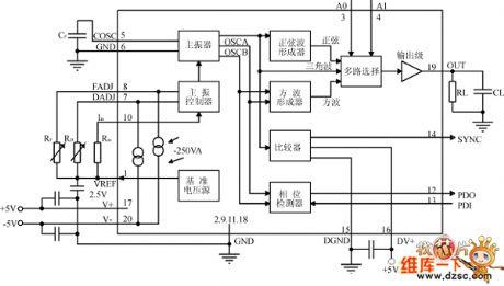
US Company Maxim develops a new function signal generator ICMAX038,which is of high-frequency,pretty-precision,and thus it is known as high frequency precise function signl generator IC.MAX038 can be the optimized module to the circuit of phase-locked loop,voltage controlled oscillator,frequency synthesizer,pulse width modulator and so on.Its inner cirucit is shown as following picture 1. (View)
View full Circuit Diagram | Comments | Reading(1480)
The electric speed regulator circuit of ceiling fans
Published:2011/6/4 3:02:00 Author:qqtang | Keyword: speed regulator, ceiling fans
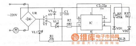
The regulator circuit consists of the power supply circuit, non-steady multi-resonate oscillator and control execute circuit, see as figure 1.
In the circuit, the power supply circuit consists of fan motor M, rectifier fridge UR, LED VLI, current limiting resistor RI, voltage diode VS and filter capacitor C1; the non-steady multi-resonate oscillator consists of time-based integrated circuit IC, resistors of R3 and R4, diodes of VD1 and VD2, potentiometer RP and capacitor C2; the control execute circuit consists of thyristor VT and LED VLZ. (View)
View full Circuit Diagram | Comments | Reading(2837)
The auto-illuminance control system circuit
Published:2011/6/2 9:12:00 Author:Seven | Keyword: auto-illuminance control system
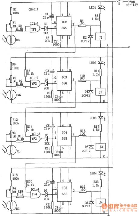
The following is an auto-illuminance control system circuit. This control system consists of 4 streams of photoelectric switch circuits. Take the first stream as an example, the light dependent resistor(LDR) is in a low resistance in the light, but it is a high resistance when the light is weak or it's dark outside. Therefore, when it's dark outside, the high voltage, which is got by the high-resistant RG, R1 and WI, flows through the NAND IC1-1(1/4 CD4011), and then it is imposed on 5-pin of IC2(555), which makes the 2-pin of IC2 to be offset due to the low LEV and the 2-pin is in a steady state, the 3-pin outputs a high LEV, the relay of J1 pulls in and relevant devices are glowing.
(View)
View full Circuit Diagram | Comments | Reading(699)
Scintillation Caution Light (8)
Published:2011/6/3 5:56:00 Author:Sue | Keyword: Scintillation, Caution, Light
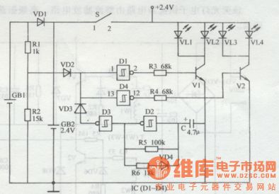
In the daytime, soler energy battery GB1 will charge GB2 through VD1. The other circuit will provide D1 and D4 with high level through VD2, and D1's andD4's output terminals will have low level. V1 and V2 are disconnected and VL1-VL4 are not illuminated.
At night, VD1 and VD2 are disconnected. GB2 will provide the circuit with working voltage. When the multivibrator begins to work, D3's output terminal will output low frequency oscillator signals which will illuminated VL1-VL4. When the signal has high level, VD3 is connected and D1's andD4's input terminals have high level and their output terminals have low level. V1 and V2 are disconnected. VL1-VL4 are not illuminated. When the signal has low level, VD3 is disconnected. V1 V2 are connected and VL1-VL4 are illuminated. (View)
View full Circuit Diagram | Comments | Reading(507)
Scintillation Caution Light (7)
Published:2011/6/3 5:57:00 Author:Sue | Keyword: Scintillation, Caution, Light
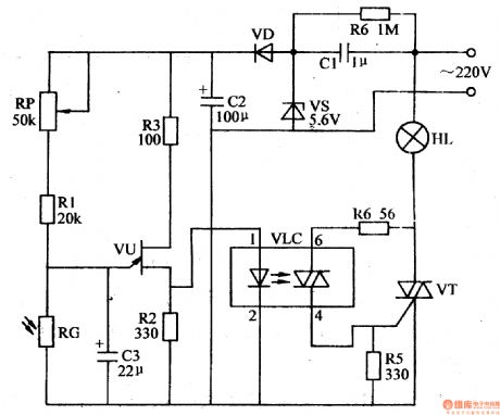
The 220V alternating current voltage will provide the oscillator with +5V working voltage after reduction, stablization, rectification and filtration.
In the daytime, RG has a low resistancevalue because of the light. C3 has a low level and the oscillator doesn't work. VLC and VT are disconnected. HL is not illuminated.
At night, RG has a high resistance value because of the lack of light. The oscillator begins to work and VLC and VT are connected intermittently. HL begins to twinkle. (View)
View full Circuit Diagram | Comments | Reading(615)
Scintillation Caution Light (6)
Published:2011/6/3 5:45:00 Author:Sue | Keyword: Scintillation, Caution, Light

In the daytime, RG has a lowresistance valuebecause of the light. D1's b terminal has a low level and the oscillator doesn't work. D1 outputs high level. D2-D4 output low level. HL1-HLn are not illuminated.
At night, RG has a high resistance value. D1's b terminal has high level and the oscillator begins to work. VLC and VT are connected from time to time, which will make HL1-HLn twinkle. When the oscillator outputs negative pulse signal, D2-D4 output high level and VLC's LED is illuminated. HL1-HLn are illuminated. When the signal is positive, D2-D4 output low level, VLC and VT are disconnected. HL1-HLn are not illuminated. (View)
View full Circuit Diagram | Comments | Reading(519)
MC1391 line oscillation PLL integrated circuit
Published:2011/6/9 2:17:00 Author:Christina | Keyword: line oscillation, PLL, integrated circuit
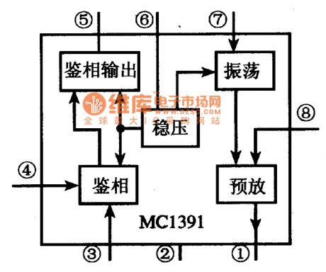
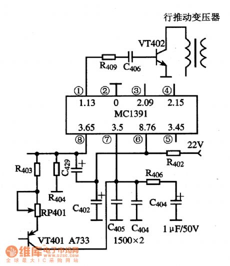
The MC1391 is designed as one kind of line oscillation PLL integrated circuit that is produced by the MOTOROLA company, it can be used in the computer color displayers such as the ASahi series color displayers.
1.Features
The MC1391 is composed of the phase discriminator, the oscillation circuit, the pre-amplifier circuit, the voltage-stabilizing circuit.etc. The internal circuit block diagram is as shown in the figure.
The internal circuit block diagram of MC1391
2.The pin functions and data of pin-5
The MC1391 uses the 18-pin dual-row DIP package, the pin functions and data are as shown in the table.
The pin functions and data of the MC1391
3.Typical application circuit
The typical application circuit of the line oscillation PLL integrated circuit which is composed of the MC1391 is as shown in the figure.
The typical application circuit of the line oscillation PLL integrated circuit which is composed of the MC1391 (View)
View full Circuit Diagram | Comments | Reading(1591)
MC3362 small power narrowband FM receiving integrated circuit
Published:2011/6/9 1:38:00 Author:Christina | Keyword: small power, narrowband, FM, receiving, integrated circuit
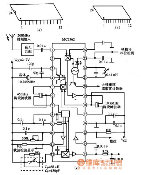
The MC3362 is designed as one kind of small power narrowband FM receiving integrated circuit that is produced by the MOTOROLA company, and it can be used in the FM receiving circuit of the narrow band audio and data communications.
1.Features
The MC3362 has two narrowband FM receiving circuit of the FM conversion oscillator and the mixer, the internal circuit is as shown in the figure (c).
2.Pin functions
The MC3362 has two packages: one is the 24-pin dual-row DIP package, as the figure (a) shows; another is the 24-pin small SMD package, as the figure (b) shows.
The internal circuit of the MC3362
3.Typical application circuit
The decoder typical application circuit which is composed of the MC3362 is as shown in the figure. The pin functions is as shown in the table.
The typical application circuit of the MC3362
The pin functions of the MC3362
(View)
View full Circuit Diagram | Comments | Reading(2127)
MC6338 fan single chip microcomputer integrated circuit
Published:2011/6/9 1:19:00 Author:Christina | Keyword: fan, single chip, microcompute, integrated circuit

The MC6338 is designed as one kind of fan single chip microcomputer integrated circuit that is produced by the MOTOROLA company, and it can be used in the fan program-controlled systems.
The MC6338 is in the 18-pin dual-row DIP package, the typical application is as shown in the figure, the pin functions and data is as shown in the table.
The typical application circuit of the MC6338
The pin functions and data of the MC6338
(View)
View full Circuit Diagram | Comments | Reading(618)
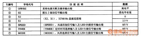
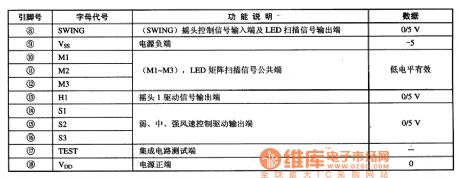
MC6805R3 air conditioner single chip microcomputer integrated circuit
Published:2011/6/9 1:13:00 Author:Christina | Keyword: air conditioner, single chip, microcomputer, integrated circuit

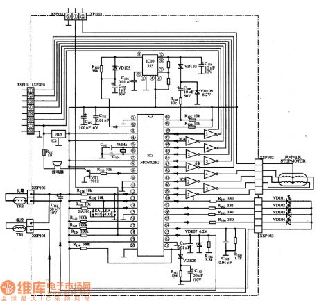
The MC6805R3 is designed as one kind of air conditioner single chip microcomputer integrated circuit that is produced by the MOTOROLA company, and it can be used in the Mitsubishi and Haier series air conditioner.
1.Pin functions
The MC6805R3 is in the 40-pin dual-row package, the pin functions are as shown in the table.
The pin functions of the MC6805R3
2.Typical application
The typical application circuit of the air conditioner control circuit which is composed of the MC6805R3 is as shown in the figure.
The typical application circuit of the MC6805R3 (View)
View full Circuit Diagram | Comments | Reading(1141)
TC9020P-003--the integrated circuit of letter display generators
Published:2011/6/7 10:45:00 Author:qqtang | Keyword: integrated circuit, letter display generator
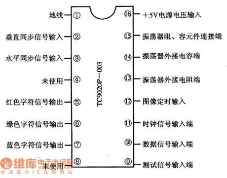
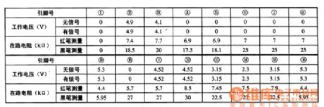
TC9020P-003 is an integrated circuit of letter display generator produced by Toshiba, which is widely used in many makes of local and imported color TV.1. Function features TC9020P-003 includes clock oscillator circuit, data input connector circuit, horizontal/vertical field locating and blank signal process circuit, etc.2.pin functions and dataTC9020P-003 is in 16-pin dual in-line package, whose pin functions are shown in Figure 1, and its parameters are listed in Table 1.Figure 1. The pin functions of TC9020P-003
(View)
View full Circuit Diagram | Comments | Reading(747)
TC9020P-011--The letter display generating integrated circuit
Published:2011/6/7 10:21:00 Author:qqtang | Keyword: letter display generating, integrated circuit
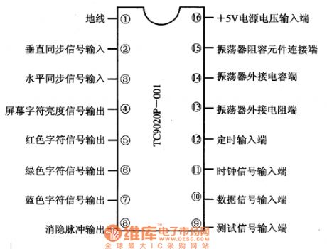
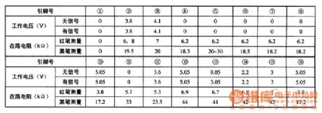
TC9020P-011 is a letter display generating integrated circuit, which is widely used in many makes of local and imported color TV.1.function featuresTC9020P-011 contains the letter signal generating circuit, clock oscillating circuit, data input connector circuit, horizontal/vertical field locating and black signal process circuit, etc. 2.pin functions and dataTC9020P-011 is in 16-pin dual in-line package, whose pin functions are in Figure 1, and the working parameters are listed in Table 1.Figure 1. pins of TC9020P-011
(View)
View full Circuit Diagram | Comments | Reading(715)
The logic probe circuit with display function
Published:2011/6/8 2:02:00 Author:qqtang | Keyword: logic probe circuit, display function
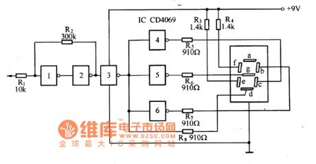
The logic probe circuit with display functionThe circuit is shown in the circuit, it consists of a 6-backward phaser integrated circuit CD4069 and LED digit displayer. The NANDs of 1,2 and 3 form a Schmidt trigger as the logic probe, which is used to measure the logic LEV directly. The Schmidt trigger circuit is fixed with two threshold LEV, by adjusting R, we can change the LEV values of the two thresholds, so that we can judge the logic LEV of the circuit under test. The NANDs of 3,4 and 5 form a decoding circuit of strokes.
(View)
View full Circuit Diagram | Comments | Reading(2018)
practical electronic switch circuit
Published:2011/6/4 9:40:00 Author:John | Keyword: electronic switch
Practical electronic switch circuit is shown below.
(View)
View full Circuit Diagram | Comments | Reading(927)
90% for the maximum duty cycle gate drive circuit
Published:2011/6/9 0:33:00 Author:John | Keyword: gate drive
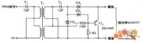
90% for the maximum duty cycle gate drive circuit is shown in the figure. The key of the circuit is the clamp circuit composed of capacitance coupling circuit and VD1. The secondary side output signal of pulse transformer Tl is positive. When the upper part is positive and the lower one is negative, the output signal leads to conduct VD2 and VD3 through C2. Such provides drive signals for the power MOSFET’s gate and drives it to turn on. When the secondary side output signal of T1 is negative, also known as that upper part is negative and the lower one is positive, VD2 and VD3 turn off due to the clamping action of VD1. VTl is saturated to conduct, leading the power MOS-FET gate’s charge to be rapidly discharged. As a result, on / off delay time for the power MOSFET has been reduced.
(View)
View full Circuit Diagram | Comments | Reading(660)
power MOSFET gate drive constituted by the transistor and others circuit
Published:2011/6/9 4:31:00 Author:John | Keyword: transistor, power MOSFET gate drive
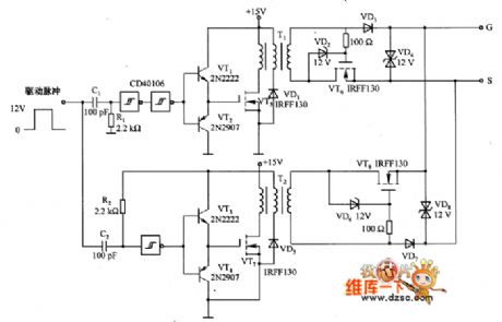
The circuit consists of two forward converters, for which one is the converter to charge the power MOSFET gate capacitor and the other is to discharge its gate capacitor. Recommended power supply voltage is from 12V to 15V. On the rising edge of the driving pulse, VT5 receives the pulse. Referring to given value for Cl and Rl in the figure, its typical duration is 2OOns. Then the pulse is transmitted to the secondary side of transformer Tl. When VT6 and VD3 are all given to a appropriate bias, the sub-pulse would charge the capacitor between the power MOSFET and the source pole. Afterwards, the current path is closed.
(View)
View full Circuit Diagram | Comments | Reading(2400)
in-phase adder circuit
Published:2011/6/9 4:39:00 Author:John | Keyword: in-phase adder
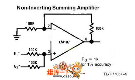
in-phase adder circuit
(View)
View full Circuit Diagram | Comments | Reading(1025)
Loom controller circuit diagram
Published:2011/5/30 6:33:00 Author:Lucas | Keyword: Loom controller
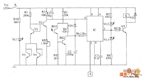
The loom controller circuit consists of touching control circuit, light control circuit, overheat protection circuit, working status indicator circuit and control implementation circuit, the circuit is shown as the chart. Touching control circuit is composed of touching electrode A and the pin 2 of time-base integrated circuit IC2. Light control circuit consists of infrared emitting diode VL1, infrared phototransistor V5, transistor V6, resistors R10 and R3 ~ R6 and the pin 7 of IC. Thermal protection circuit consists of transistors V1 ~ V4, diode VD1, resistors R1 and R2, capacitors C1 and C2, potentiometer RP and pin 6 of the internal IC. Control implementation circuit is composed of the transistor V7, relay K, resistor R9 and diode VD2. Working status indicator circuit consists of resistors R7, R8 and LEDs VL1, VL2.
(View)
View full Circuit Diagram | Comments | Reading(812)
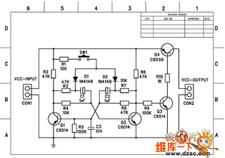
Herald M810 amplifier system control circuit( two)
Published:2011/6/5 0:02:00 Author:John | Keyword: amplifier
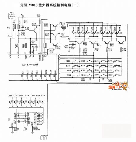
Herald M810 amplifier system control circuit( two) is shown below.
(View)
View full Circuit Diagram | Comments | Reading(699)
| Pages:253/312 At 20241242243244245246247248249250251252253254255256257258259260Under 20 |
Circuit Categories
power supply circuit
Amplifier Circuit
Basic Circuit
LED and Light Circuit
Sensor Circuit
Signal Processing
Electrical Equipment Circuit
Control Circuit
Remote Control Circuit
A/D-D/A Converter Circuit
Audio Circuit
Measuring and Test Circuit
Communication Circuit
Computer-Related Circuit
555 Circuit
Automotive Circuit
Repairing Circuit