
Measuring and Test Circuit
Index 55
RF_WATTM_ETER
Published:2009/7/8 2:11:00 Author:May
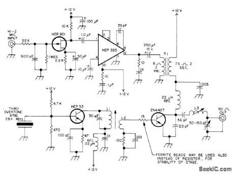
Calibration is accurate on all HF bands because circuit is not frequency-sen-sitive. Sensitivity depends on metermovement, number of turns in primary coil, and resistive voltage divider. With values shown, pots can be adjusted for full-scale values from 1-14 W. C1 and C2 are 3-20 pF. Diodes are 1N34A, 1N60, or equivalent. L1 is 46 turns No. 28 on Amidon T-50-2 toroid, with 2 turns No. 22 between ends of L1 for L2. To adjust, connect resistive dummy load to one coax receptacle and RF power source to other, with R2 at maximum resistance.Place upper switch in position providing high-est meter reading, and make that the FWD position. Switch to other position, which becomes REF, and adjust C1 for null reading. Reverse RF source and load, leaving switch at FWD, and ad-iust C2 for null. Wattmeter can now be cali-brated.—A. Weiss, ORP Low-Low Power Opert ating, CQ Jan. 1974, p 42-44 and 80. (View)
View full Circuit Diagram | Comments | Reading(1859)
BREATH_MONITOR
Published:2009/7/8 2:07:00 Author:May
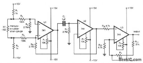
The mercury-in-rubber strain gauge is the detector of breathing. In the model device, the strain gauge produced by Meclimatic, Demark was used. The change in the length of the strain gauge wrapped around the chest during breathing causes a varying electrical resistance of about 0.2 Ω/cm. The constant current passing R1, RT and R4 gives the constant component on the output of U1 differential amplifier. The change in the resistance of the strain gauge, which results from breathing, produces proportional varying in output voltage of U1 amplifier. The voltage follower, based on U2, separates the output voltage of the filter from the input stage amplifier. U3 works as a noninverter amplifier with regulated gain. This device should be supplied with a stabilized constant voltage of ±15 V. (View)
View full Circuit Diagram | Comments | Reading(1768)
PEAK_dB_METER
Published:2009/7/8 2:02:00 Author:May

This circuit compares a rectified input,VNN, with a voltage that decays exponentially across a 4.7-kΩ resistor and a 0.01-μF capacitor.Comparing the exponentially decaying voltage with the rectified input provides a peak-level indication that requires no adjustment.A phaes-locked loop controls the scan rate so that each LED represents 6 dB in the 30 dB range. (View)
View full Circuit Diagram | Comments | Reading(922)
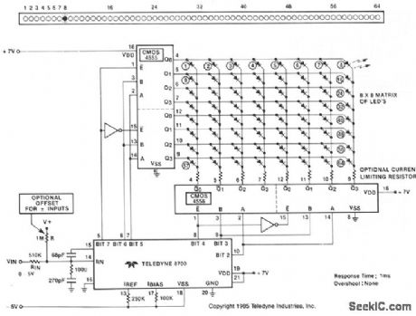
LED_PANEL_METER
Published:2009/7/8 1:59:00 Author:May
View full Circuit Diagram | Comments | Reading(1959)
SOUND_LEVEL_METER
Published:2009/7/8 1:53:00 Author:May
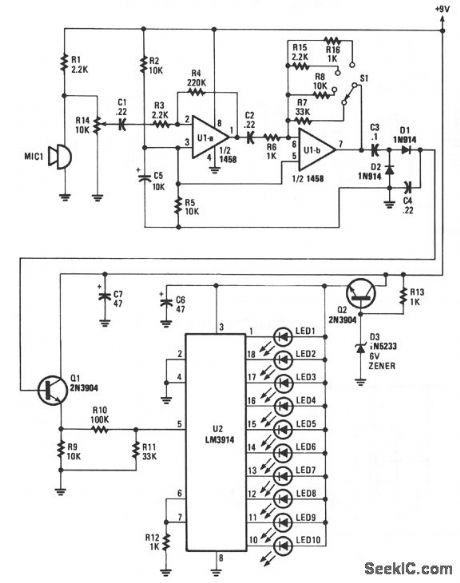
Sounds are picked up by MIC1 and fed to the input of the first op amp. The signal is then fed to the input of second op amp U1b, where it is boosted again by a factor of between 1 and 33, depending upon the setting of range switch S1.
With the range switch set in the A position, R6 is 1 KΩ and R7 is 33 KΩ, so that stage has a gain of 33.In the B position, the gain is 10Ω; in the C position, the gain is 22Ω; and in the D position the gain is 1 Ω.
As the signal voltage fed to the input of U2 at pin 5 varies, one of ten LEDs will light to correspond with the input-voltage level. At the input's lowest operating level, U2 produces an output at pin 1, causing LED1 to light. The highest input level presented to the input of U2, about 1.2 V, causes LED10 to turn on. (View)
View full Circuit Diagram | Comments | Reading(1)
SIMPLE_CONTINUITY_TESTER
Published:2009/7/8 1:51:00 Author:May
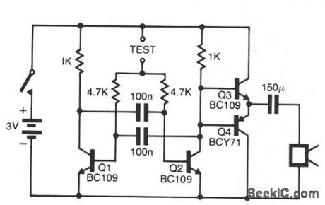
The pitch of the tone is dependent upon the resistance under test. The tester will respond to resistances of hundreds of kilohms, yet it is possible to distinguish differences of just tens of ohms in low-resistance circuits. Q1 and Q2 form a multivibrator, the frequency of which is influenced by the resistance between the test points. The output stage, Q3 and Q4, will drive a small loudspeaker or a telephone earpiece. The unit is powered by a 3-V battery, and draws very little current when not in use.
(View)
View full Circuit Diagram | Comments | Reading(0)
TEMPERATURE_MEASURING_ADD_ON_FOR_DMM_DIGITAL_VOLTMETER
Published:2009/7/8 1:50:00 Author:May
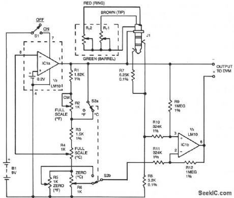
The DVM-to-temperature adapter is built around a single IC, National's LM10. That micropower IC contains a stable 0.2 V reference, a reference amplifier and a general-purpose op amp. The circuit is designed for a linear temperature range of 0 to 100 °C (32 to 212 °F). The 0.2-V reference and reference amplifier provide a stable, fixed-excitation voltage to the Wheatstone bridge. The voltage is determined by a feedback network consisting of R1 through R6. Switch S2a configures the feedback to increase the voltage from 0.6 V on the Celsius range to 1.08 V on the Fahrenheit range. These differences compensate for the fact that one degree Fahrenheit produces a smaller resistance change than does one degree Celsius.Resistors R1 through R16 also form the fixed leg of the Wheatstone bridge, nulling the bridge output at zero degrees. Since 0 °C is different from 0 °F, S2b is used to select the appropriate offset.The LM10's op amp, along with R9 through R12, form a differential amplifier that boosts the bridge output to 10 mV per degree. Since a single supply is used, and since the output must be able to swing both positive and negative, the output is referenced to the bridge supply voltage, rather than to the common supply. (View)
View full Circuit Diagram | Comments | Reading(1105)
_DIGITAL_FREQUENCY_METER
Published:2009/7/8 1:48:00 Author:May
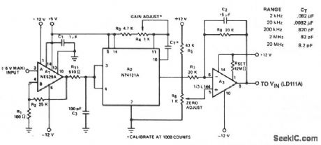
The circuit converts frequency to voltage by taking the average dc value of the pulses from the 74121 monostable multivibrator. The one shot is triggered by the positive-going ac signal at the input of the 529 comparator. The amplifier acts as a dc filter, and also provides zeroing. This circuit will maintain an accuracy of 2% over 5 decades of range. The input signal to the comparator should be greater than 0.1 V pk-pk, and less than 12 V pk-pk for proper operation. (View)
View full Circuit Diagram | Comments | Reading(2222)
_SCR_TESTER
Published:2009/7/8 1:46:00 Author:May
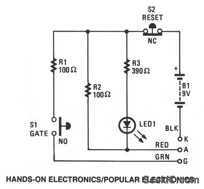
The DUT's(Device Under Test) cathode, anode, and gate are connected to the unit's K,A, and G terminals, respectively. Pressing switch S1 feeds a gate current to the DUT, which triggers it on. Resistor R1 limits the gate current to the appropriate level. Resistor R3 limits the current through the LED to about 20 mA, which, with the current through R2, results in a latching current of about 110 mA. The LED is used to monitor the latching current. If the DUT is good, once the gate is triggered with S1, the LED will remain lit, indicating that the device is conducting. To end the test, turn off the device by interrupting the latching current flow using switch S2. The LED should turn off and remain off. The preceding procedure will work with SCRs and triacs. To check LEDs and other diodes, connect the anode and cathode leads to the anode and cathode of the diode; LED1 should light.When the leads are reversed, the LED should remain off. (View)
View full Circuit Diagram | Comments | Reading(1148)
AUDIBLE_LOGIC_TESTER
Published:2009/7/8 1:45:00 Author:May
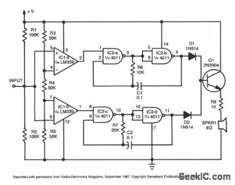
This tester provides an audible indication of the logic level of the signal presented to its input. A logic high is indicated by a high tone, a logic low is indicated by a low tone, and oscillation is indicated by an alternating tone. The input is high impedance, so it witt not load down the circuit under test. The tester can be used to troubleshoot TTL or CMOS logic. The input consists of two sections of an LM339 quad comparator. IC1a increases when the input voltage exceeds 6770 of the supply voltage. The other comparator increases when the input drops below 330/0 of the supply.
The tone generators consist of two gated astable multivibrators. The generator built around IC2a and IC2b produces the high tone. The one built around IC2c and IC2d produces the low tone. Two diodes, D1 and D2, isolate the tone-generator outputs. Transistor Q1 is used to drive a low-impedance speaker.
(View)
View full Circuit Diagram | Comments | Reading(0)
S_METER
Published:2009/7/8 1:41:00 Author:May
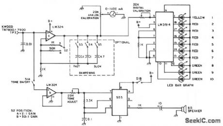
This design is for an external signal strength meter that is analog, digital, and audible for mobile trans-mitter hunters. The S meter also incorporates a gain circuit. The digital LED bar graph display has a very fast response time. The 3.3-KΩ resistor near LM3914 can be replaced with a 5-K pot to control LED brightness. The 52A position gives a 2:1 gain and the 52B position gives about a 50:1 gain. The calibration pots control the amount of meter action relative to the gain. The optional dampening circuit is used for the averaging of a transmitted signal that has modulated power or when a dip on the voice peaks occur. The capacitors can be switched one 'oy one or switched into a very slow response using 5.8 μF total capacitance.
(View)
View full Circuit Diagram | Comments | Reading(3660)
_LINE_CURRENT_MONITOR
Published:2009/7/8 1:39:00 Author:May
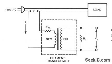
A low-cost ftlament transformer provides a linear indication of the load current in an ac line. This method causes a slight series voltage drop over a wide range of load currents. (View)
View full Circuit Diagram | Comments | Reading(755)
MOTOR_HOUR_METER
Published:2009/7/7 23:18:00 Author:May
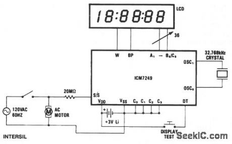
In this application, the ICM7249 is conftgured as an hours-in-use meter and shows how many whole hours of line voltage have been applied. The 20-MΩ resistor and high-pass ftltering allow ac line activation of the S/S input. This configuration, which is powered by a 3-V lithium cell, will operate continuously for 21/2 years. Without the display, which only needs to be connected when a reading is required, the span of operation is extended to 10 years.
(View)
View full Circuit Diagram | Comments | Reading(0)
ELECTROSTATIC_DETECTOR
Published:2009/7/7 23:09:00 Author:May
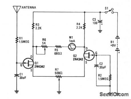
The heart of the electroscope is the two junction FETs Q1 and Q2 connected in a balanced-bridge circuit. The gate input of Q1 is connected to the wire pick-up antenna, while Q2's gate is tied to the circuit's common ground through R2. That type of bridge circuit offers excellent temperature stability; therefore, Q1 is allowed to operate in an open-gate configuration. Potentiometer R7 is used to balance the bridge circuit, and R6 sets the maximum meter swing. Capacitors C1 and C2 help to reduce the 60-Hz pickup and add to the short-term stability of the circuit. (View)
View full Circuit Diagram | Comments | Reading(2301)
TACHOMETER_AND_DIRECTION_OF_ROTATION_CIRCUIT
Published:2009/7/7 23:05:00 Author:May
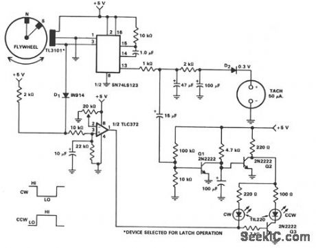
In machine and equipment design, some applications require measurement of both the shaft speed and the direction of rotation. Fig. 56-4 shows the circuit of a tachometer, which also indicates the direction of rotation. The flywheel has two magnets embedded in the outer rim about 45° apart. One magnet has the north pole toward the outside and the other magnet has the south pole toward the outside rim of the flywheel. Because of the magnet spacing, a short on pulse is produced by the TL3101 in one direction and a long on pulse in the other direction. A 0-50 μA meter is used to monitor the flywheel speed while the LEDs indicate the direction of rotation. The direction-of-rotation circuit can be divided into three parts:
· TLC372 device for input conditioning and reference adjustment.· Two 2N2222 transistors which apply the VCC to the two LEDs when needed.· The two TTL 220 LEDs which indicate clockwise (CW) or counterclockwise (CCW) direction of rotation. (View)
View full Circuit Diagram | Comments | Reading(1177)
WIDE_RANGE_RF_POWER_METER
Published:2009/7/7 22:58:00 Author:May


The Hewlett-Packard HSCH-3486 zero-bias Schottky diode is used as the detector.To avoid using a modulation method of detection,a chopper-stabilized op amp is used.The chopper op amp basically converts the mput dc voltage to ac,amplifiesit,and converts it back to dc.Amplifying the dc output from the detector 150 times with a chopper opamp puts the signal at a level that simpler op amps,such as the LM11,can handle, Offset voltages hthe amplifier are nulled with two pots one for the lower three ranges. (View)
View full Circuit Diagram | Comments | Reading(1457)
RING_DETECTOR
Published:2009/7/7 22:45:00 Author:May
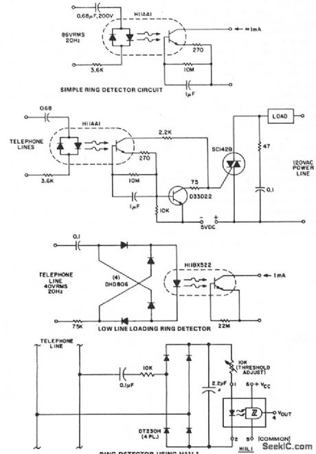
This circuit detects the 20 Hz, ≈ 86-V rms ring signal on telephone lines and initiates action in an electrically isolated circuit. Typical applications would include automatic answering equipment, and interconnect/interface and key systems. The circuits illustrated are bare bones circuits designed to illustrate concepts. They might not eliminate the ac/dc ring differentiation, 60-Hz noise rejection, dial tap rejection, and other effects that must be considered in field application. The first ring detector is the simplest and provides about 1-mA signal for a 7-mA line loading for 1/10 sec after the start of the ring signal. The time delay capacitor provides a degree of dial tap and click suppression, as well as filtering out the zero crossing of the 20-Hz wave. This circuit provides the basis for a simple example, a ring extender that operates lamps and buzzers from the 120-V, 60-Hz power line, while maintaining positive isolation between the telephone line and the power line. Use of the isolated tab triac simplifies heat sinking by removing the constraint of isolating the triac heatsink from the chassis. Lower line current loading is required in many ring detector applications. This can be provided by using the H11BX522 photo-Darlington optocoupler, which is specified to provide a 1-mA output from a 0.5-mA input through the -25°C to +50°C temperature range.°The next circuit allows ring detection down to a 40-V rms ring signal while providing 60-Hz rejection to about 20-V rms. Zero-crossing filtering can be accomplished either at the input bridge rectifier or at the output. Dependable ring detection demands that the circuit responds only to ring signals, rejecting spurious noise of similar amplitude, such as dialing transients. The configuration shown relies on the fact that ring signals are composed of continuous frequency bursts, whereas dialing transients are much lower in repetition rate. The dc bridge-filter combination at the H11L input has a time constant; it cannot react to widely spaced dialing transients, but will detect the presence of relatively long duration bursts, causing the H11L to activate the downstream interconnect circuits at a precisely defined threshold. (View)
View full Circuit Diagram | Comments | Reading(0)
PHASE_SENSITIVE_DETECTOR
Published:2009/7/7 22:36:00 Author:May
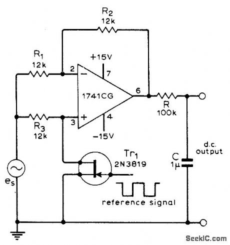
Circuit using single opamp produces DC output proportional to both amplitude of AC input signal and cosine of its phase angle relative to reference signal.Can be used as synchronous rectifier in chop-per-type DC amplifier or for accurate measurement of small AC signals obscured by noise. Article gives design equations.-G. B. Clayton, Experiments with Operational Amplifiers, Wire-less World, July 1973, p 355-356. (View)
View full Circuit Diagram | Comments | Reading(0)
DUTY_CYCLE_MONITOR
Published:2009/7/7 22:29:00 Author:May
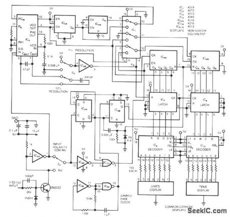
The circuit monitors and displays a digital signal's duty cycle and provides accuracy as high as ±1%.Using switch S2, you can choose a frequency range of either 250 Hz to 2.5 kHz at ±1% accuracy or 2 kHz to 50 kHz at ±10% accuracy. The common-cathode display gives the signal's duty-cycle percentage.Phase-locked loop IC4 and counters IC5A and IC5B multiply the input frequency by a factor of either 10 or 100, depending on switch S2's setting. IC6A and IC6B count this multiplied frequency during the incoming signal's mark interval. IC7 and IC8 then latch this count and display it at the clock's sample rate. For example, if you select a 1% resolution, when the signal's mark period is 40% of the total period, the circuit will enable the counter comprising IC6A and IC6B for 40 counts. To obtain space-interval sampling, you can reverse the input polarity using switch 51. IC2A samples the input signal's period and enables gate IC2C and resets the counter. IC2E and IC2F form the sample-rate clock; IC3B synchronizes the clock's output with the input, so that the circuit can update latches IC7 and IC8.
(View)
View full Circuit Diagram | Comments | Reading(1903)
OUTPUT_LIMITER
Published:2009/7/7 22:21:00 Author:May
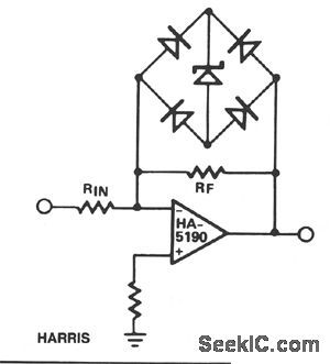
HA-5190 is rated for ±5 V output swing, and saturates at ±7 V. As with most op amps, recovery from output saturation is slow compared to the amplifier's normal response time. Some form of limiting, either of the input signal or in the feedback path, is desirable if saturation might occur. The circuit illustrates a feedback limiter, where gain is reduced if the output exceeds ± ( Vz + 2 Vf). A 5-V zener with a sharp knee characteristic is recommended. (View)
View full Circuit Diagram | Comments | Reading(879)
| Pages:55/101 At 204142434445464748495051525354555657585960Under 20 |
Circuit Categories
power supply circuit
Amplifier Circuit
Basic Circuit
LED and Light Circuit
Sensor Circuit
Signal Processing
Electrical Equipment Circuit
Control Circuit
Remote Control Circuit
A/D-D/A Converter Circuit
Audio Circuit
Measuring and Test Circuit
Communication Circuit
Computer-Related Circuit
555 Circuit
Automotive Circuit
Repairing Circuit