
Circuit Diagram
Index 1579
Signal Wire Protection Circuit
Published:2011/7/10 8:16:00 Author:Robert | Keyword: Signal Wire, Protection
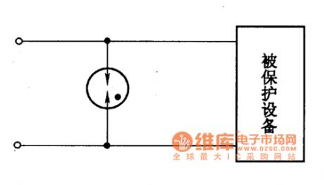
Generally the signal wire would not be connected to ground when it is running. If take a two-polar gas discharging tube to connected between the two signal wires of the protected equipment, it could protect the equipment before the differential surge voltage damage the equipment, which shows in the picture.
The picture shows the signal wire protection circuit. (View)
View full Circuit Diagram | Comments | Reading(581)
555 Multivibrator Circuit
Published:2011/7/8 9:49:00 Author:Robert | Keyword: Multivibrator
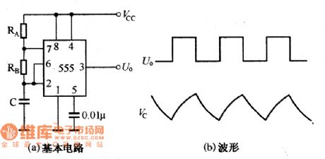
By using the 555 time-base circuit it can make up many kinds of self-excited multivibrator and its basic circuit is shown in picture a. When the circuit is firstly connected to the power, the C has not been charging in time, the 555 circuit's pin 2 is at low voltage level. This makes its pin 3 output high voltage level. When the C is in the status of Vc≥Vcc, which is charged by the power through RA and RB, the pin 3 output port would be changed from high voltage level to low voltage level. And the capacitor C would discharge through the RB and internal circuit's discharging switch tube. When it is discharged to Vc≤Vcc, the output port would be changed from low voltage level to high voltage level again. At this time the capacitor would be charging again. This process would cycle to proceed and it would form the self-excited oscillation. The picture (b) shows the waveform of voltage on the output port and capacitor C. (View)
View full Circuit Diagram | Comments | Reading(1380)
555 Time-Base Circuit Internal Structure Circuit
Published:2011/7/8 21:25:00 Author:Robert | Keyword: Time-Base, Internal, Structure
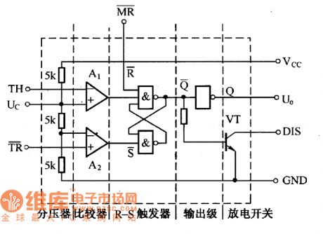
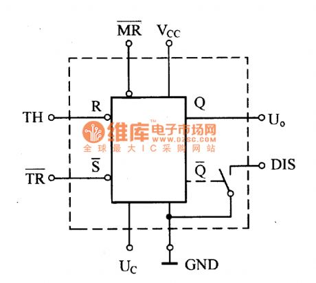
The 555 time-base circuit is divided into two categories which are TTL type and CMOS type. The picture shows the TTL type circuit's internal structure circuit. From the picture we notice that it is made up of voltage divider, comparator, R-S trigger, output stage and discharging switch and so on. The comparator's main function in the circuit is to compare the input voltage to the reference voltage formed by the voltage divider. And it would show the comparing result by outputing high voltage level 1 or low voltage level 0 in its output port. The 555 circuit's R-S trigger is made up of two NAND gates with cross connection. In order to reset the R-S trigger to zero directly, the trigger is lead to a MR port. It could simply set the MR port to low voltage level 0 , the trigger would be set to zero immediately which means Q=0=Uo, no matter what original status the trigger has and no matter what signal the trigger's input port is added. So the MR port is also known as the total-reset port. (View)
View full Circuit Diagram | Comments | Reading(1487)
Frequency / voltage conversion circuit composed of analog switch
Published:2011/7/6 20:02:00 Author:Lucas | Keyword: Frequency conversion , voltage conversion , analog switch
The circuit has improved the monostable circuit and the switching circuit with higher precision conversion, and it can switch 12 to 24Hz frequency signal to 0 to -lV voltage signal.
(View)
View full Circuit Diagram | Comments | Reading(704)
the internal equivalent circuit of NJM4200 multiplier
Published:2011/7/10 3:44:00 Author:chopper | Keyword: internal, equivalent circuit, multiplier
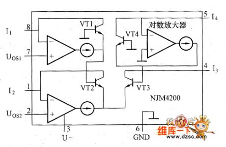
Figure shows the internal equivalent circuit of NJM4200, and the chip includes logarithmic amplifiers and so on. Function of the Logarithmic amplifier is to use the logarithmic relationship of voltage and current of PN,and add and subtract logarithm of current,then do the logarithmic transformation for the result.The transition function of NJM4200 is I3=(I1I2)/I4,and the input/output range is 1μA~1mA.NJM4200 may be damaged when the input current is more than 5mA,while the frequency characteristics is poor when small signal level is in use,therefore, we should use it near the full-scale as possible as we can.
(View)
View full Circuit Diagram | Comments | Reading(914)
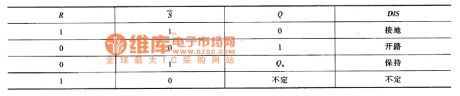
Frequency / voltage conversion circuit composed of TA7506
Published:2011/7/6 20:00:00 Author:Lucas | Keyword: Frequency conversion, voltage conversion
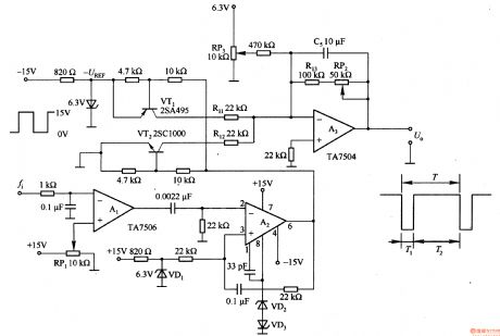
Al is the waveform shaping circuit, and A2 is the monostable multivibrator,then it gets a constant pulse width T2. VT1, VT2 and A3 constitute a frequency / voltage conversion circuit. In the T2 period, VTl turns on and integrates -U (REF) voltage; in the T1 period, VTl ends and VT2 conduction, the integrator A3 input voltage is OV. The C5, R3 and RP2 form low-pass filter, so A3 output is DC voltage. Adjusting the value of RP3 make fi = 12Hz, U. = OV; adjusting RP2 value make fi = 24Hz, U. = LV.
(View)
View full Circuit Diagram | Comments | Reading(834)
Pulse width / voltage conversion circuit composed of μPC157
Published:2011/7/7 22:17:00 Author:Lucas | Keyword: Pulse width conversion, voltage conversion
After the input end is addedthe negative pulse, A1 starts integrate. The input pulse inversion is in high level, to sample and keep the output of the integrator. After sampling, the integrator resets. Repeat this operation, we can obtain the output pulse width which is proportional to the output voltage.
(View)
View full Circuit Diagram | Comments | Reading(884)
Voltage / frequency conversion circuit composed of TC4013
Published:2011/7/7 22:12:00 Author:Lucas | Keyword: Voltage conversion, frequency conversion
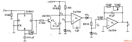
It can switch 0-100Hz input frequency to 0 -l0V output voltage. In the circuit, TC4013 is a monostable multivibrator, which could shape and amplify input pulse, and the input pulse width is 1OOμs. TC4013 could trigger VTl to turn on, when the input voltage of of comparator Al UQ <UR, its output is positive. VTl is only conducted in 10Oμs, then returned to the cut-off state, and capacitor Cl starts charging. When the charging voltage of C1 is up to UQ> UR, Al output becomes negative.
(View)
View full Circuit Diagram | Comments | Reading(3071)
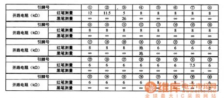
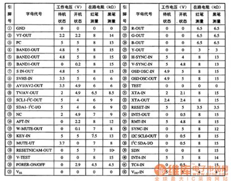
CPU6527 Single-Chip Micro-Computer Integrated Circuit
Published:2011/7/8 9:26:00 Author:Robert | Keyword: Single-Chip, Micro-Computer, Integrated
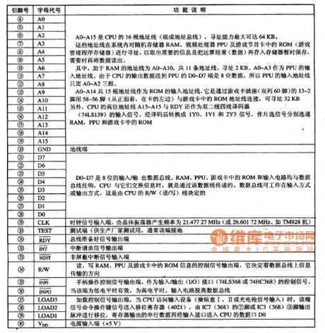
The CPU6527 is a single-chip micro-computer IC which is widely used in game devices.
1.Its functional features.
The CPU6527 IC's internal part is mainly made up of central processing unit (CPU), clock oscillation circuit, reset circuit, input/output data bus interface circuit, loading control circuit, address bus interface circuit, RAM memory circuit, interrupt request control circuit, handle operation control circuit, reading/writing control circuit, testing circuit, analog audio signal processing circuit, power circuit and other some auxiliary function circuit and so on.
2.Its pin's function and data.
The CPU6527 uses 40-pin dual inline plastic package and it is a 8-bit NMOS VLSI. Its pin's function is listed in table 1 and its open-circuit resistance is listed in table 2. (View)
View full Circuit Diagram | Comments | Reading(694)
HY-100 Series Music Integrated Circuit
Published:2011/7/8 21:59:00 Author:Robert | Keyword: Music, Integrated
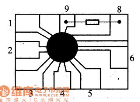
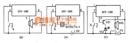
1. The HY-100 series music integrated circuit.
The HY-100 series music IC is a large-scale CMOS IC. This circuit integrates the total circuit, which includes the preamplifier and power amplifier circuit, to a 25mmx15mm PCB by using the CMOS technology. This chip has been soldered a 68kΩ resistance which is shown in the picture.
The picture shows the HY-100 series music IC.
The HY-100 series IC has the features of big driving capacity and flexible output port operation. Its pin 5 is power output port which can drive the loudspeaker directly. Its pin 3, pin 4 are preamplifier's output ports which can drive the piezoelectric buzzer working and driving the semiconductor diode. The HY-100 series music IC is a circuit can be used as doorbell. When the positive pulse triggers the pin 2 trigger port, it would play the music sound automatically about 20s. (View)
View full Circuit Diagram | Comments | Reading(1341)
KD-156 Music Integrated Circuit
Published:2011/7/8 21:38:00 Author:Robert | Keyword: Music, Integrated
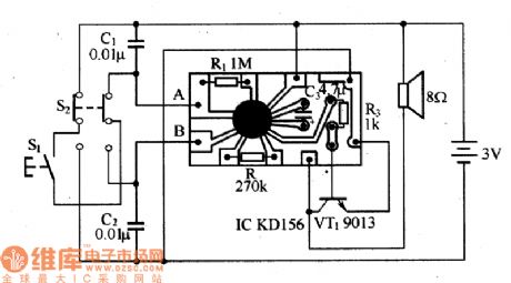
The KD-156 music IC can play the Ding-Dong and birds singing these two sounds. Its sounds are pure and sweet and it is a special IC to be used to make the electronic doorbell. The electronic doorbell circuit made by using this IC is shown in the picture. The A, B ports in the picture are two trigger signal input ports. A is positive pulses trigger port and B is negative pulses trigger port. S1 is button switch and S2 is selection switch. When the S2 is set in position shown in the picture, by pressing the S1 the A port would be connected with the power positive source. And the IC would be triggered to output the birds singing signal. By amplification through VT1, the loudspeaker would play the birds singing sound. If the S2 is set to the other position, when pressing S1, the B port would be connected with the power nagetive source and would get negative pulses trigger signals. With the action of the trigger signal, the loudspeaker would play twice the Ding-Dong sound. (View)
View full Circuit Diagram | Comments | Reading(1981)
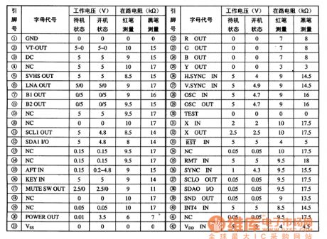
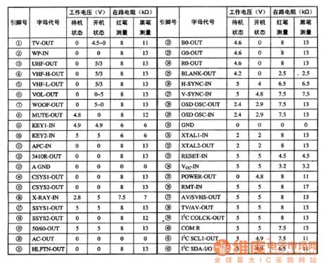
CKP1301S Single-Chip Micro-Computer Integrated Circuit
Published:2011/7/8 10:30:00 Author:Robert | Keyword: Single-Chip, Micro-Computer, Integrated
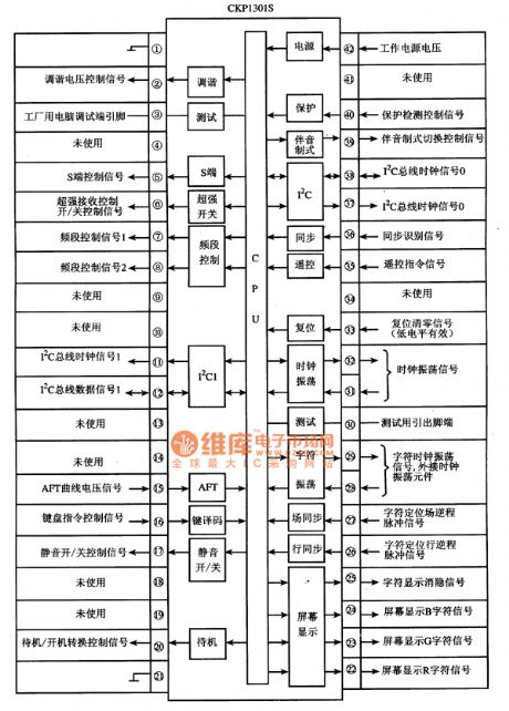
The CKP1301S is a single-chip micro-computer IC which is widely used in Konka series large screen color TV sets.
1.Its functional features.
The CKP1301S IC's internal part is mainly made up of central processing unit (CPU), clock oscillation circuit (main clock, screen display oscillation clock), reset control circuit, I2C bus control circuit, key command signal decoding circuit, remote-control command signal processing circuit, screen display character generating and processing circuit, standby/starting control circuit, testing circuit, sound system switch circuit and other some control and auxiliary function circuits and so on. Its internal circuit diagram and pin's function and signal flowing is shown in picture 1.
The picture 1 shows the CKP1301S IC's internal circuit diagram and pin's function and signal flowing.
2.Its pin's function and data.
The CKP1301S IC uses 42-pin dual package. Its pin's function is shown in picture 1 and its pin's letter code and data is listed in table 1.
The table 1 is shows the CKP1301S IC's pin's letter code and data. (View)
View full Circuit Diagram | Comments | Reading(572)
CKP1105SA Single-Chip Micro-Computer Integrated Circuit
Published:2011/7/8 23:44:00 Author:Robert | Keyword: Single-Chip, Micro-Computer, Integrated
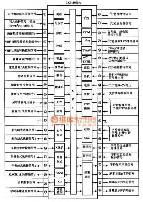
The CKP1105SA is a single-chip micro-computer IC which is widely used in many kinds of screens of the Konka series color TV sets.
1.Its functional features.
The CKP1105SA IC's internal part is made up of CPU, clock oscillation circuit (main clock, screen displaying clock), reset control circuit, I2C bus control circuit, key command signal decoding circuit, remote-control command signal processing circuit, standby and starting control circuit, screen display character generating and processing circuit, squelch control circuit, TV/AV switch control circuit and other some control and auxiliary function circuits and so on. Its internal circuit diagram and pin's function and signal flowing is shown in picture 1.
The picture 1 shows the CKP1105SA IC's internal circuit diagram and pin's function and signal flowing.
2.Its pin's function and data.
The CKP1105SA IC uses 42-pin dual package. Its pin's function is shown in picture 1 and its pin's letter code and data is listed in table 1.
The table 1 shows the CKP1105SA IC's pin's letter code and data. (View)
View full Circuit Diagram | Comments | Reading(862)
UCC3580 converter circuit
Published:2011/7/10 5:49:00 Author:chopper | Keyword: converter circuit
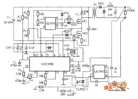
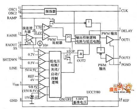
Figure 1 shows the UCC3580 converter, and it is the positive driving DC-DC converter whose input voltage is +18~+30 V, and output is 5V/8A. In the circuit, the control circuit adopts UCC3580 integrated controller,and the internal equivalent circuit is shown as Figure 2.In the UCC3580 there is the oscillator which can determine the switching frequency and dead time,error amplifier, pulse by pulse type over-current protection circuit,PWM control comparator,the circuit which can decide the work starting voltage and stopping voltage,and the PWM output which can drive the main switch and auxiliary switch and timing circuits and so on.
(View)
View full Circuit Diagram | Comments | Reading(1289)
CKP1008S Single-Chip Micro-Computer Integrated Circuit
Published:2011/7/8 23:59:00 Author:Robert | Keyword: Single-Chip Micro-Computer Integrated Circuit
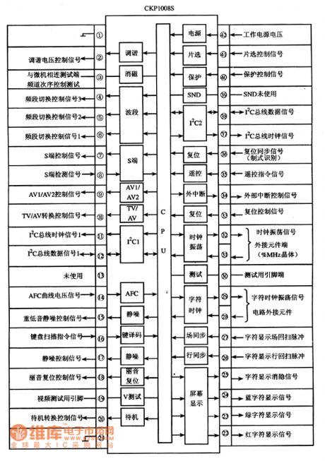
The CKP1008S is a single-chip micro-computer IC which is widely used in many kinds of screens of the Konka series color TV sets.
1.Its functional features.
The CKP1008S IC's internal part is made up of CPU, reset control circuit, clock oscillation circuit, key command decoding circuit, I2C bus control circuit, standby switch control circuit, screen display character generating and processing circuit, remote-control command signal processing circuit, testing circuit, TV/AV switch circuit and other some control and auxiliary function circuits and so on. Its internal circuit diagram and pin's function and signal flowing is shown in picture 1.
The picture 1 shows the CKP1008S IC's internal circuit diagram and pin's function and signal flowing.
2.Its pin's function and data.
The CKP1008 IC uses 42-pin dual package. Its pin's function is shown in picture 1 and its pin's letter code and data is listed in table 1.
The table 1 shows the CKP1008 IC's pin's letter code and data. (View)
View full Circuit Diagram | Comments | Reading(534)
LT1725 converter circuit
Published:2011/7/10 5:37:00 Author:chopper | Keyword: converter circuit
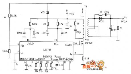
Figure shows the LT1725 converter,and this is the isolated DC-DC converter whose input voltage is +48V,and output is +5V/2A.As for the LT1725 integrated controller,it can obtain output voltage of high stability even if it is without negative feedback from the secondary side.And it has fewer external components,the circuit is relative simple.
(View)
View full Circuit Diagram | Comments | Reading(1658)
IX1083AFZZ IC Internal Circuit Diagram And Typical Application Circuit
Published:2011/7/8 10:48:00 Author:Robert | Keyword: IC, Internal, Diagram, Application
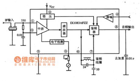
The IX1083AFZZ is a FM middle amplifier and frequency-discriminator IC produced by the Japanese SHARP company. It is widely used in car audio, home audio and other kinds of audio systems.
The IX1083AFZZ IC uses the three-stage differential middle-frequency amplifier and differential peak-value wave detector, and it has adjustable squelch and squelch point. It has few external connected elements and has a stable signal voltage-level driving circuit. Its working voltage's range would be 8-15V. Its internal circuit diagram and typical application circuit is shown in the picture.
The picture shows the IX1083AFZZ IC's internal circuit diagram and typical application circuit. (View)
View full Circuit Diagram | Comments | Reading(588)
current limiting circuit
Published:2011/7/10 4:00:00 Author:chopper | Keyword: current, limiting circuit
current limiting circuitis shown as picture
(View)
View full Circuit Diagram | Comments | Reading(737)
UC3843A converter circuit
Published:2011/7/10 5:32:00 Author:chopper | Keyword: converter circuit
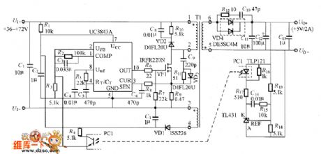
Figure shows the UC3843A converter,and it is the 5V/2A isolated flyback-type converter. This is the equivalent circuit of UC3843A whose input voltage is +36 ~+72 V,and output is shown as the picture.
(View)
View full Circuit Diagram | Comments | Reading(9966)
IX0986CE IC Internal Circuit Diagram And Typical Application Circuit
Published:2011/7/9 0:17:00 Author:Robert | Keyword: IC, Internal, Diagram, Application
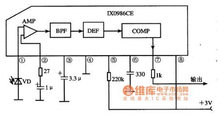
The IX0986CE is a remote-control signal receiving IC produced by the Japanese SHARP company. It is used widely in the remote-control systems in the SHARP company's many kinds of electronic products, such as the color TV sets.
The IX0986CE IC has internal infrared signal receiving preamplifier circuit, band-pass filter circuit, wave detection circuit, output buffer amplification circuit and other some auxiliary function circuits and so on.
The remote-control signal receiving typical application circuit composed of K0986CE IC is shown in the picture.
The picture shows the IX0986CE IC's internal circuit diagram and typical application circuit. (View)
View full Circuit Diagram | Comments | Reading(544)
| Pages:1579/2234 At 2015611562156315641565156615671568156915701571157215731574157515761577157815791580Under 20 |
Circuit Categories
power supply circuit
Amplifier Circuit
Basic Circuit
LED and Light Circuit
Sensor Circuit
Signal Processing
Electrical Equipment Circuit
Control Circuit
Remote Control Circuit
A/D-D/A Converter Circuit
Audio Circuit
Measuring and Test Circuit
Communication Circuit
Computer-Related Circuit
555 Circuit
Automotive Circuit
Repairing Circuit