
Circuit Diagram
Index 1562
basic application circuit of YDS-100T series DC-DC converter
Published:2011/7/8 20:33:00 Author:chopper | Keyword: basic application , DC-DC converter
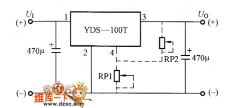
basic application circuit of YDS-100T series DC-DC converter is shown as picture
(View)
View full Circuit Diagram | Comments | Reading(574)
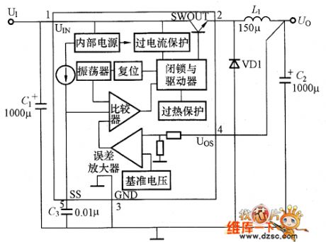
YDS-105-S2 basic application circuit
Published:2011/7/8 20:34:00 Author:chopper | Keyword: basic, application circuit

YDS-105-S2 basic application circuit is shown as picture
(View)
View full Circuit Diagram | Comments | Reading(1048)
ZCS switching power supply circuit of NE555
Published:2011/7/8 20:44:00 Author:chopper | Keyword: ZCS, switching, power supply
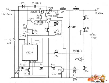
The picture shows the ZCS switching power supply circuit of NE555.This is the current resonance method(ZCS) switching power supply which is formed by adding LC series resonant circuit to step-down DC-DC converter.ZCS mode adopts fixed conduction time of resonant cycle-time to change frequency modulation.In the circuit, NE555 forms the common step-down DC-DC converter composed of voltage-controlled oscillators,switching power MOSFET (VF1),freewheeling diode YD3,smoothing inductor L2 and so on.Inductor L1, capacitor C2 constitute a resonant circuit. (View)
View full Circuit Diagram | Comments | Reading(3495)
DC power supply circuit
Published:2011/7/8 20:56:00 Author:chopper | Keyword: DC, power supply
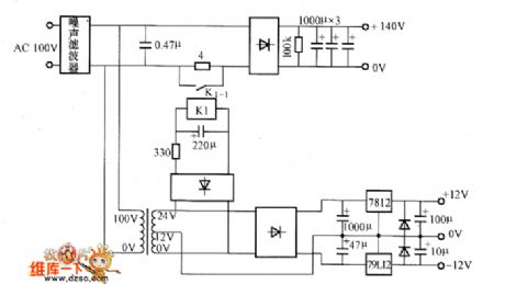
Figure shows the DC power supply circuits. AC 100V voltage is converted into a 140V DC voltage after it is commutated by the bridge rectifier and smoothed by smoothing capacity (3 1000μF capacitor in parallel), and the DC voltage is the main circuit power supply. AC 100V voltage offer stable ±12V power supply for control circuit after it is steped down by transformer,commutated by the bridge rectifier and smoothed by smoothing capacity,then regulated by 7812 and 79L12.The circuit adopts relay K1 to prevent impulse current at the moment when the power is connected.At this time,the relay K1 will stop contact K1-1, and add 4 Ω current-limiting resistor to the circuit.
(View)
View full Circuit Diagram | Comments | Reading(921)
grid drive circuit and full bridge output circuit
Published:2011/7/8 21:00:00 Author:chopper | Keyword: grid drive, full bridge, output circuit
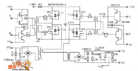
Figure shows the grid drive circuit andfull bridge output circuit.As for the phase shift type PWM circuit,duty ratio of grid drive wave is always 50%,so it is very easy to use pulse transformer in the drive circuit.
(View)
View full Circuit Diagram | Comments | Reading(729)
UCC3895N phase shift control circuit
Published:2011/7/8 21:08:00 Author:chopper | Keyword: phase shift, control circuit
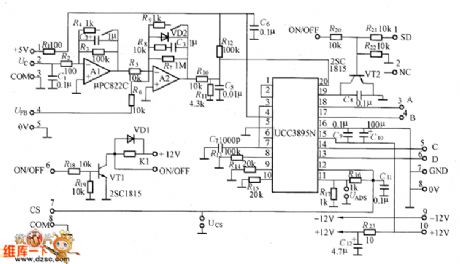
Figure shows the UCC3895N phase shift control circuit,and in order to reduce the interference of the power switching circuit, it can substrate the control circuit.Uc control input voltage of ② end of left placode can offer 0~+5V voltage by connecting 5V benchmark voltage of UCC3895N to 10kΩ adjustable resistor,can also use D/A converter to generate the control voltage. It can not join capacitor Ca in order to speed up response time. (View)
View full Circuit Diagram | Comments | Reading(1603)
UCC3895N internal equivalent circuit
Published:2011/7/8 21:09:00 Author:chopper | Keyword: internal, equivalent circuit
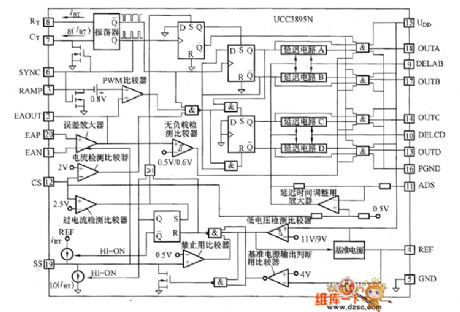
View full Circuit Diagram | Comments | Reading(956)
traditional PWM control full-bridge circuit
Published:2011/7/9 3:12:00 Author:chopper | Keyword: traditional, PWM control, full-bridge circuit
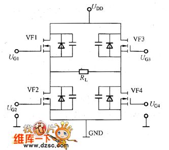
Figure shows a traditional PWM control full-bridge circuit and waveforms of control signal. As for 4 switches in the circuit,VF1 and VF4 will conduct meanwhile(positive output), and VF2 and VF3 will conduct meanwhile(negative output). Change the conduction and close time of switch tube as well as duty ration to control the output voltage.
(View)
View full Circuit Diagram | Comments | Reading(749)
high efficiency solar special charge management upgrating circuit-CN3083
Published:2011/7/6 7:07:00 Author:chopper | Keyword: high efficiency, solar, special charge management, upgrating circuit
Overview : CN3083 is a single lithium battery charge management chip which can be powered with solar panels.The device includes power transistor,and its application does not require the external current detection resistor and blocking diode.Internal 8-bit analog - digital conversion circuit can automatically adjust the charge current by the current output capability of input voltage supply.Users do not need to consider the worst case.It can maximize the use of the current output capability of input voltage soupply which is ideal for lithium battery charge application powered by solar panels whose current output capacity is limited. (View)
View full Circuit Diagram | Comments | Reading(1097)
low power quad voltage monitor integrated circuit--CN1185
Published:2011/7/6 6:55:00 Author:chopper | Keyword: low power, quad voltage monitor, integrated circuit
Overview : CN1185 is a low power quad voltage monitor chip,its current consumption is only 7.3 microamps,so it is ideal for monitoring battery voltage.Chip contains four voltage comparators.And the positive input end of each comparator is connected to the voltage benchmark source in the inner chip,which can be used to monitor four different voltage source or voltage source for the same grade monitoring. Users can choose the flip threshold and comparator hysteresis of the comparators by logical input port. (View)
View full Circuit Diagram | Comments | Reading(1041)
5W high-power LED driving circuit--CN5612
Published:2011/7/6 6:41:00 Author:chopper | Keyword: 5W, high-power, LED, driving circuit
overview:
CN5612 is a current modulation circuit under 2.7V-6V voltage,and constant output current is up to 1.2A.It can be used to drive various LEDs including white LEDs.The current of the LED terminal of CN5612 is through an external resistor to set the current range of 30mA to 1.2A.In the inner integrated chip there are power transistors,thus greatly it reduces the number of external components.Other functions include chip over-temperature protection, LED short / open circuit protection. CN5612 adopts 5-pinned TO252 package with good cooling capacity. (View)
View full Circuit Diagram | Comments | Reading(1412)
1W high power LED driving circuit--CN5611
Published:2011/7/8 3:03:00 Author:chopper | Keyword: 1W, high power, LED, driving circuit
Overview : CN5611 is a current modulation circuit under 2.7V to 6V,its constant output current is up to 800mA, and it can be used to drive various LEDs including white LEDs.Current on the LED end of CN5611 is through an external resistor to set the current range of 30mA to 800mA. Integrated chip contains power transistors,which greatly reduces the number of external components.Other functions include chip over-temperature protection, LED short/open circuit protection. CN5611 adopts 5 pinned SOT89 package whose cooling capacity is good. (View)
View full Circuit Diagram | Comments | Reading(1266)
high efficiency 1000MA current charger management circuit--CN3056
Published:2011/7/8 6:06:00 Author:chopper | Keyword: high efficiency, 1000MA current, charger management
Overview :CN3056 is a charger circuit which can charge rechargeable batteries like single quarter lithium ion or lithium-polymer in constant current/voltage mode.The device includes power transistor,and its application does not require the external current detective resistor and blocking diode.CN3056 only requires few external components, and works under USBbus technologyspecifications,thus it is ideal for portable applications.Heat modulation circuit can control the chip temperature within safety range if the power consumption of devices is bigger or the environmental temperature is higher.
(View)
View full Circuit Diagram | Comments | Reading(892)
Solar special USB compatible charging management circuit of high efficiency--CN3063
Published:2011/7/8 3:25:00 Author:chopper | Keyword: Solar, special, USB compatible, charging management, high efficiency
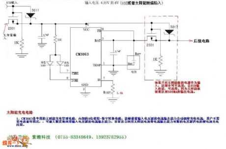
Overview :CN3063 is a single lithium battery charge management chip which can be powered with solar panels.The device includes power transistor,and its application does not require the external current detective resistor and blocking diode.The internal 8-bit analog-digital conversion circuit can automatically adjust the charge current by the current output capability of input voltage supply.Users need not consider the worst case, and it can maximize the use of the current output capability of input voltage supply.
(View)
View full Circuit Diagram | Comments | Reading(2914)
SI-8000S inner equivalent circuit
Published:2011/7/8 6:12:00 Author:chopper | Keyword: inner, equivalent circuit
SI-8000S inner equivalent circuit is shown as picture
(View)
View full Circuit Diagram | Comments | Reading(713)
Practical digital amplifier (TL084) circuit
Published:2011/7/6 5:42:00 Author:chopper | Keyword: Practical, digital amplifier
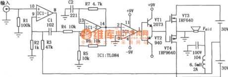
Conventional home theater digital amplifier requires the special integrated circuit, but such a integrated circuit has few manufacturers,and the high price. The circuit can be made by common components, and power is 50W.There is no power consumption when it is no-load,full load efficiency is about 85%,thus it has a certain practical value.However,the final stage of its power supply adopts floating ground ,the electromagnetic compatibility of the circuit is poor. As the 200kHz carrier does not filter out cleanly, its distortion and the signal to noise ratio and other indicators are still to be improved. (View)
View full Circuit Diagram | Comments | Reading(7534)
TDA2822,TDA2822M Double audio power amplifier integrated circuit
Published:2011/7/5 8:53:00 Author:chopper | Keyword: Double, audio power amplifie, integrated circuit
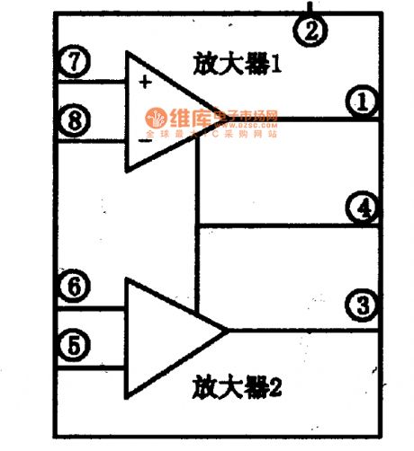
TDA2822 IC has a small quiescent current and cross-distortion characteristics,and it can be composed of dual-channel BTL circuit which is suitable for portable, miniature tape recorders, PC audio to be the power amplifier.1.The inner circuit and function of pins of TDA2822 integrated packageThere are two packages of integrated circuit: TDA2822 adopts 16-pin dual inline package structure, and TDA2822M adopts 8-pin package structure,their internal equivalent circuits are basical the same. The inner circuit of TDA2822 integrated package is shown as the picture(take TDA2822M for example)
(View)
View full Circuit Diagram | Comments | Reading(2281)
multimedia Hi-Fi power amplifier circuit
Published:2011/7/5 6:36:00 Author:chopper | Keyword: multimedia, Hi-Fi, power amplifier circuit
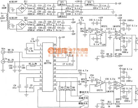
This circuit is a active power amplifier to listen Hi-Fi music on a PC, as picture shown. Audio processing chip ICl adopts uniwafer QS7779 virtual surrounding circuit produced by Canadian QSOUND company.Because the circuit includes Dolby prologic and Dolby digital mixed signal decoder,thus,first,it can improve the normal stereo signal effect;second, when it plays a DVD Dolby digital signal,it can be decoded firstly, then the matrix computing, virtualization before outputting from the two-channel; three,it can present different effects by switch.
(View)
View full Circuit Diagram | Comments | Reading(4825)
TA8164P-AM/FM former stage radio integrated circuit
Published:2011/7/5 8:44:00 Author:chopper | Keyword: AM/FM, former stage, radio, integrated circuit
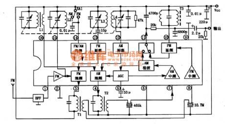
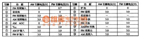
TA8164P is a former stage radio integrated circuit,and it is applied to radio system like low-voltage radio,tape recorder .1.The inner circuit and function of pins of TA8164PTA8164P integrated package includes AM high level circuit, local oscillator circuit, mixing circuit,medium level circuit and detector circuit;FM high-level, local oscillator, mixing, medium level,frequency discriminating circuit; and ACC circuit, FM / AM band selection circuit. The inner circuit and typical application circuit of integrated circuit are shown as picture 1.
(View)
View full Circuit Diagram | Comments | Reading(5344)
Swedish Leica card laser rangefinder
Published:2011/7/6 7:09:00 Author:chopper | Keyword: swedish, Leica card, laser rangefinder
View full Circuit Diagram | Comments | Reading(485)
| Pages:1562/2234 At 2015611562156315641565156615671568156915701571157215731574157515761577157815791580Under 20 |
Circuit Categories
power supply circuit
Amplifier Circuit
Basic Circuit
LED and Light Circuit
Sensor Circuit
Signal Processing
Electrical Equipment Circuit
Control Circuit
Remote Control Circuit
A/D-D/A Converter Circuit
Audio Circuit
Measuring and Test Circuit
Communication Circuit
Computer-Related Circuit
555 Circuit
Automotive Circuit
Repairing Circuit