
Circuit Diagram
Index 1564
ABS Circuit One of Southeast LingShuai Cars
Published:2011/7/7 21:09:00 Author:Michel | Keyword: LingShuai Cars, ABS Circuit One
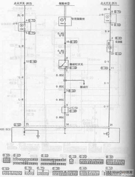
View full Circuit Diagram | Comments | Reading(438)
ABS Circuit Two of Southeast LingShuai Cars
Published:2011/7/7 21:11:00 Author:Michel | Keyword: LingShuai Cars, ABS Circuit Two
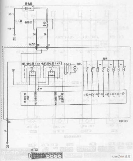
ABS Circuit of Southeast LingShuai Cars (View)
View full Circuit Diagram | Comments | Reading(432)
ABS Circuit Three of Southeast LingShuai Cars
Published:2011/7/7 21:12:00 Author:Michel | Keyword: LingShuai Cars, ABS Circuit Three
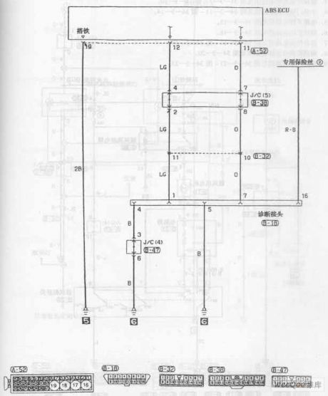
ABS Circuit of Southeast LingShuai Cars (View)
View full Circuit Diagram | Comments | Reading(443)
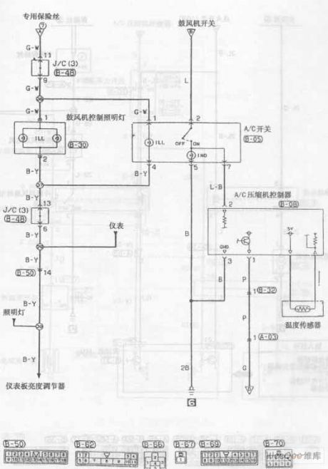
Air-conditioning Circuit One of Southeast LingShuai Cars
Published:2011/7/7 21:16:00 Author:Michel | Keyword: LingShuai Cars, Air-conditioning Circuit One
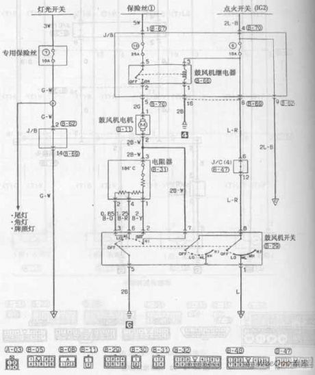
Air-conditioning Circuit of Southeast LingShuai Cars (View)
View full Circuit Diagram | Comments | Reading(684)
Air-conditioning Circuit Two of Southeast LingShuai Cars
Published:2011/7/7 21:18:00 Author:Michel | Keyword: LingShuai Cars, Air-conditioning Circuit Two
Air-conditioning Circuit of Southeast LingShuai Cars (View)
View full Circuit Diagram | Comments | Reading(766)
Single Output (Unbalanced output) Differential Amplifier Circuit
Published:2011/6/25 9:17:00 Author:Michel | Keyword: Single Output, Unbalanced output, Differential Amplifier Circuit
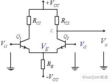
When Vo was taken out by point C of the Q1 and Q2,it is called single ended or single ended.Single ended is one time smaller than differential output.The common mode signal can not be suppressed when the signal ended outputs. because Vi1 and Vi2 increase meanwhile ,VC1 and VC2 reduce,what's more,Vo=VC2 but it is not zero(generating zero-point drift).But increasing RE resistance can increase negative back to suppress output and common-mode signals. Because when Vi1=Vi2 ,Ii1 and Ii2 increase at the same time,IE and VE increase,which makes Q1 and Q2 generate reverse feedback and Q1 and Q2 gain and loss reduce,that's to say Vo reduces.
(View)
View full Circuit Diagram | Comments | Reading(2209)
Disinfectant Manufacturer (the 1st)
Published:2011/7/7 10:09:00 Author:Felicity | Keyword: Disinfectant Manufacturer, the 1st
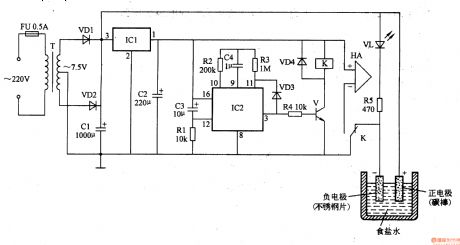
Work of the circuit
The disinfectant manufacturer circuit consists of power circuit, timing circuit, controlling circuit, acousto-optic circuit and electrodes. (It is showed in picture 9-92.).
Turn on the power and 220V AC voltage produces +7.5V voltage after being reduced rectified and filtered by T, VD1, VD2 and CI. The voltage then separates into three parts. One is directly supplied on the positive electrode and one is supplied to IC2, electric relay K and annunciator HA while another is supplied to electrode VL.
When the regular time (usually 1 hour) is reached, the annunciator HA will work to remind the users that the disinfectant is done. (View)
View full Circuit Diagram | Comments | Reading(553)
Fan Speed Control Circuit of MAX1626
Published:2011/6/26 7:01:00 Author:Michel | Keyword: Fan, Speed Control, Circuit
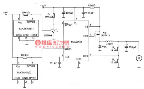
The aboved picture is fan speed control circuit composed of MAX1626.This circuit reduces the computer, the temperature controller and alarm system noise and power consumption by choosing the MDH626 shut-off and the output voltage function. Logic level is added to 2 (3 V / 5 V) and 3 (SHDN) pins and at the same time,feedback resistance (Rl and R2) are chosen to set the output voltage.Usually, a low output voltage U (01) (here it's eight V) is determined by dividing resistor R1 and R2.High output voltage U (02) here it's l2V) is determined by chip the output (4 feet) voltage.When environment temperature is more than the threshold values within the chip, the MAX6501 (1) and (2) leakage output(TOVER) of monitoring temperature becomes low PWL. (View)
View full Circuit Diagram | Comments | Reading(858)
Helmets with Electronic Hearing Aids
Published:2011/7/10 23:30:00 Author:Felicity | Keyword: Helmets, Electronic Hearing Aids,
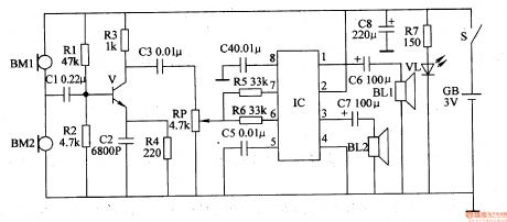
When the motorcycle drivers wear their helmets their hearing will be limited and it is very dangerous. But if the drivers wearthis kind ofhelmets with electronic hearing aids their hearing will be improved and the accidents will be reduced.
Work of the circuit
Turn on the power switch S and VL will be lightened. Then the machine is in work. BL1 and BL2 turn the sound singnal they have collected into electronic singnal and transit the singnal to V's base through C1. The singnal will drive BL1 and BL2 to make sound after being preamplified by V, volume controlled by RP and power amplified by IC. (View)
View full Circuit Diagram | Comments | Reading(4279)
SR03× Driving White LED Circuit
Published:2011/6/23 11:19:00 Author:Michel | Keyword: Driving, White LED Circuit
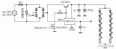
SR03 x series are dual output DC/DC power management chips without any magnetic components and the typical application circuit is shown as the aboved picture.SR036 and SR037 are two kinds of SR03 x series products of Supertex company.SR03 x series products do not need any transformer and inductor, also do not need input capacitance via high voltage,meanwhile,its work principle is very simple.SR03 x input HVin acceses rectifying 120 V or 230 V voltage of the high voltage port and it controls an external N channel mosfets or IGBT tube.The external transistor starts to conduct and charge the capacitance as the Vsource boosts when the input voltage is lower than 45V.Once when the HVin voltages is above 45 V, the external transistor will shuts off, stops charging, capacitance begins to discharge to load and maintains stable load current. (View)
View full Circuit Diagram | Comments | Reading(1113)
R1211 Driving White LED Circuit
Published:2011/6/23 11:01:00 Author:Michel | Keyword: Driving, White, LED Circuit
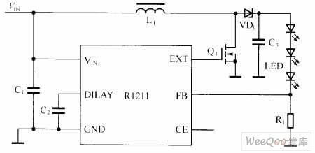
Ricoh company manufacturing R1211 series products uses the CMOS technology, is a the low power switch type boost converter of current control function.Peripheral circuit is simple and it just need a inductance, a diode, a field effect tube, and several resistance and capacitance.Its input voltage range is 2.5~5.5V which is applied to single quarter lithium ion battery or ordinary dry battery power supply occasion.The chip inside uses PWM way and it produces as much as 15 V output voltage which can drive three series LED.
R1211 series chip adopts phase compensation circuit application feedback loop which makes the boost conversion process response faster and the output voltage become more stable.The biggest R1211 duly ratio is 90%.Chip insdie builds soft start function and delay time is about 10 ms. (View)
View full Circuit Diagram | Comments | Reading(643)
MAX6964 Driving White LED Circuit
Published:2011/6/23 10:36:00 Author:Michel | Keyword: Driving, White LED Circuit
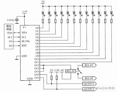
MAX6964 is a kind of I2C compatible serial interface peripheral circuit and it provide micro controller 17 output ports. The output absorbs the drain current open structure and is allowed to work in 50 mA / 7 V conditions which can drive LED or provide logic output through external voltage boost.MAX6964 inside has integrated a eight PWM current control circuit and four were global control which is used in all LED and outputs are used in current broad tuning.There are 14 brightness levels from it completely shuts off to it fully opens.In addition, every output also has independent four control bits, but the global current set is divided into 16 levels.As another choice, current control can also be configured to single eight control way, all the output can be set at a time. (View)
View full Circuit Diagram | Comments | Reading(849)
NE555 Overvoltage and Overcurrent Protection Circuit
Published:2011/6/23 10:10:00 Author:Michel | Keyword: Overvoltage, Overcurrent, Protection Circuit
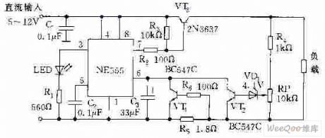
The picture is the overvoltage and overcurrent protection circuit composed of NE555. VT1 and VT ends, NE555 resets, and all of the transistor is in conduction mode.It absorbs current from VT3 which makes VT stay in saturation condition and 5~12V DC power supply provides load via VT3.When load current exceeds rating value and voltage on RS increases which makes VT1 conduct and NE555 be triggered and then VT3 stops,load power supply cuts off.At the time,NE555 is in monostable condition and NE555 is triggered again VT3 continuely isolates load from power supply as long as the load flow does not rule out. (View)
View full Circuit Diagram | Comments | Reading(3028)
110V/220V AC Voltage Automatic Switch-over Circuit
Published:2011/6/22 9:52:00 Author:Michel | Keyword: 110V/220V, AC Voltage, Automatic Switch-over, Circuit
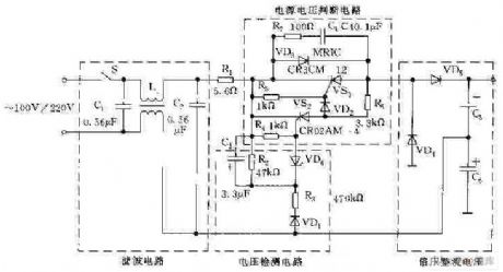
The picture is 110V/220V AC automatic switch-over circuit.When input AC voltage is 110V,charging voltage of the voltage test circuit's capacitance C3 is lower than voltage regulator tube VD6's stable voltage,V2 and thyristor VS2 shuts off ,VS1 conducts via R3 and VD2's trigger.Besides,diode VD3 is anti-paralleled with VS1 thus the latter level rectifier circuit works normally.C4 charging voltage is higher than V7 and VS2 conducts when the input voltage is 220V.As a result,None of current flows through VS1's gate level and the switch keeps off condition.The latter level times voltage turns to half wave rectifier circuit. (View)
View full Circuit Diagram | Comments | Reading(4855)
Simple Circuit of Clock Phase Adjustment
Published:2011/6/22 7:03:00 Author:Michel | Keyword: Clock Phase Adjustment, Simple Circuit
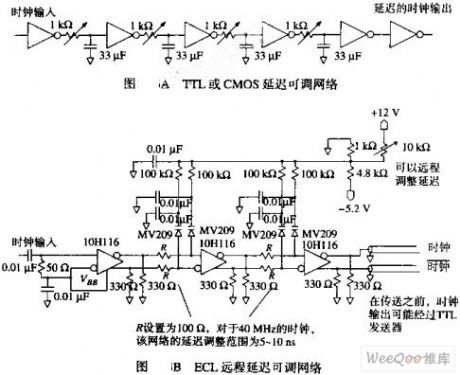
The picture shown in picture A is a hexadecimal inverter which is used to generate 30~160NS delay.Delay time of every level is 5~35NS and its value depends on variable resistance value.Delay time of every level should not be over 12% of the clock cycle to ensure stable work.
The circuit's dutyfactor can be adjusted and reaches the mininmum value by adjusting the delay levels (2 or 4) and adjusting every level resistance.It's better to adjust the shape by using an opposite phase at least at the end of the circuit before the signal entering the system.
The weakness of the circuit shown in picture A is that the circuit is the signal must pass the potentiometer. (View)
View full Circuit Diagram | Comments | Reading(748)
Time Relay (the 1st)
Published:2011/7/7 9:49:00 Author:Felicity | Keyword: Time Relay, the 1st
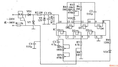
Work of the circuit
The circuit consists of +12V power circuit, oscillating circuit, delayed trigging circuit and electronic switch circuit. (It is showed in the picture 8-135.)
+12V power circuit consists of resistors Rl-R3, KA relay coil, diode VDl, voltage regulator diode VS and filter capacitor Cl.
Oscillating circuit consists of NAND gate IC IC (Dl-D6) within the non-gate D5, D6 and capacitor C2, resistors R4-R6, potentiometer RPl, diode VD2.
Delayed trigging circuit consists of lC internal NAND gate Dl, D2, D4, resistor Rg, potentiometer RP2, RP3, capacitor C3 and diode VD3.
Electronic switch circuit consists of relay KA, thyristor VT, resistors R7, R8 and capacitor C4. (View)
View full Circuit Diagram | Comments | Reading(889)
6-way infrared remoter controller circuit without no debugging
Published:2011/7/9 10:09:00 Author:Lena | Keyword: 6-way, infrared, remoter controller, no debugging
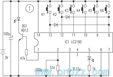
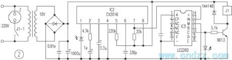
Here introduces a remote controller that consists of transmitting and receiving parts.Transmitting circuit is with LC2190 as the core, K1-K6 are coding switchs, C2 is a pulse interval timing capacitance. Modulated coding signal is outputted by IC1 ① pin, then be amplified by BG1, and be emitted by load infrared LED. The principle is shown figure 1.Receiving circuit is shown in figure 2. Encoding signal transmitted by remote controller is sent to LC2200 by IC2 CX20106, then LC2200 outputs control various ways load, A-F are related K1-K6 control output ends.
(View)
View full Circuit Diagram | Comments | Reading(994)
Loom Controller
Published:2011/7/7 2:32:00 Author:Felicity | Keyword: Loom Controller
Work of the circuit The circuit consists of touch control circuit, the light control circuit, overheat protection circuit, working status indication circuit and control implementation circuit. (It is showed in picture 8-132.) Touch control circuit consists of touching electrodes A and the circuit inside 2 feet of time-base integrated circuit IC. The light control circuit consists of infrared emitting diode VLl, infrared phototransistor, V5, transistor V6, resistors RlO and R3-R6 and circuit within IC’s pin 7. Overheat protection circuit consists of transistor Vl-V4, diode VD1, resistors Rl and R2, capacitor Cl and C2, potentiometer RP and circuit within IC’s pin 6. Working status indication circuit consists of resistors R7, R8 and LED VLl, VL2. Control implementation circuit consists of transistor V7, relay K, resistor R9 and diode VD2. (View)
View full Circuit Diagram | Comments | Reading(983)
Temperature PID Control Circuit of Operational Amplifier
Published:2011/6/22 6:41:00 Author:Michel | Keyword: Operational Amplifier, Temperature, PID Control Circuit
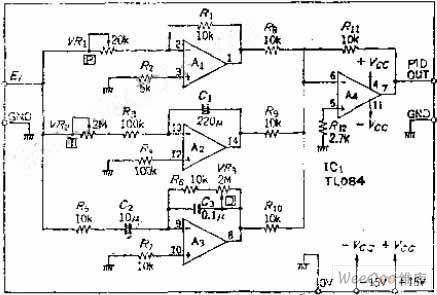
Error integral circuit can be added to the ordinary proportional control circuit if the temperature is controlled and it reaches specified value in the shortest time.But the error will increases as time goes on,the differentiating element is added to the circuit to reduce the error and increase speed and it make quick response to rapid changing temperature and the control is called PID contorl.This circuit form has high accuracy control and it is widely used.
Circuit's Work PrincipleP represents proporation circuit and it's relevant to loop gain.The variable resistance VR1 can change between 0.5~∞ by using the opposite phase the amplifier gain A.
(View)
View full Circuit Diagram | Comments | Reading(6449)
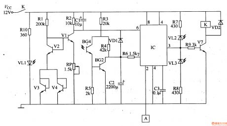
Dangerous Area Warning Device (the 3rd)
Published:2011/7/7 9:49:00 Author:Felicity | Keyword: Dangerous Area Warning Device, the 3rd
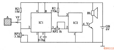
Work of the circuit
The circuit consists of sensing electrodes A, JFET VF, time-base integrated circuit ICl, language integrated circuit IC2, audio amplification V and speaker BL.(It is showed in the picture 8-123.)
When no one is near to the pole A, the resistance between VF’s drain and source is low. And the value of thee current is large. The level of IC1’s pin 2 is lower than Vcc/3. The alarm does not work.
Change the value of RP1 and RP2 to change the sensitivity of the circuit. If someone is within the distance of 0.5m to the pole, the alarm works. (View)
View full Circuit Diagram | Comments | Reading(591)
| Pages:1564/2234 At 2015611562156315641565156615671568156915701571157215731574157515761577157815791580Under 20 |
Circuit Categories
power supply circuit
Amplifier Circuit
Basic Circuit
LED and Light Circuit
Sensor Circuit
Signal Processing
Electrical Equipment Circuit
Control Circuit
Remote Control Circuit
A/D-D/A Converter Circuit
Audio Circuit
Measuring and Test Circuit
Communication Circuit
Computer-Related Circuit
555 Circuit
Automotive Circuit
Repairing Circuit