
Circuit Diagram
Index 1573
Telephone hands-free circuit
Published:2011/7/9 0:23:00 Author:Fiona | Keyword: hands-free
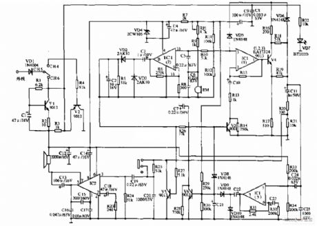
Telephone hands-free circuit is shown as above, this picture is HA22 (VI) P/TD type telephone hands-free circuit produced by jiangsu.When the telephone is in h-f state,the receiver is replaced by speaker; The microphone is replaced by sound power converter(the pickup) BM. hands-free circuit is composed of IC1, IC2 six transistor (9013) and so on. When the switch CH5 and CH6 are linked together,hands-free indicator VD7 is bright, the telephone enters into the h-f state, when CH5,CH4 are linked together or off-hook, the hands-free circuit is closed.
(View)
View full Circuit Diagram | Comments | Reading(2251)
Regulator, DC-DC circuit, power supply monitor pin and main features MC33129 and other control circuits
Published:2011/7/10 10:44:00 Author:Lucas | Keyword: Regulator, DC-DC circuit, power supply monitor, pin
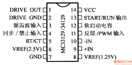
MC33129/34129 current mode switching regulator control circuit
It is the current mode switching regulator control circuit. Its output stage is the Totem form. Its supply voltage ranges from 4.2V to 12V. The maximum working frequency is 300 kHz. The maximum Zener current between the VCC terminal and START / RUN OUT side equals to 50mA. Its output current is 1.0A and ambient temperature is 70 ℃. The retention rate for mini package is 552mW. The DIP is 800mW. MC34129 works within 0 ~ +70 ℃. It contains the maximum peak switch current’s soft starting function inside, as well as low input voltage protection’s liver function. Besides, it includes over-current protection circuit with pulse lock function. (View)
View full Circuit Diagram | Comments | Reading(802)
Current / voltage conversion circuit composed of FET
Published:2011/7/6 5:08:00 Author:Lucas | Keyword: Current conversion , voltage conversion , FET
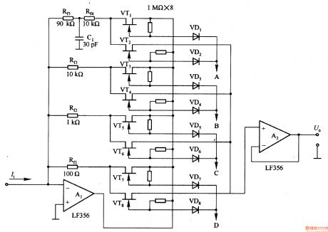
In the circuit, FET tube can switch feedback resistor Rf according to the size of the measured current to make output voltage be the specified value. The input signal is swicthed from DC signal to the lKHz AC signal with conversion accuracy in 0.1%. The accuracy of the feedback resistor and open-loop gain of Al affects the conversion accuracy. Al uses LF356, when the frequency is 1KHz, its open-loop gain is 3x1Ox1Ox1O to reach 0.1% conversion accuracy completely. A, B, C, D are switching control signal input ends.
(View)
View full Circuit Diagram | Comments | Reading(612)
Pulse width / voltage conversion circuit composed of TL082
Published:2011/7/5 8:16:00 Author:Lucas | Keyword: Pulse width , voltage conversion
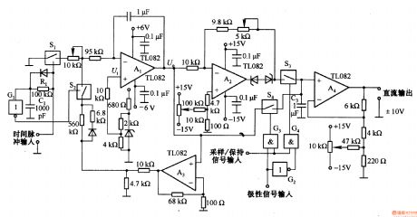
This is the pulse width (time) / voltage conversion circuit, according to the diagram component parameters, it can convert 0.1 S pulse width into 10V output voltage. When time pulse input end is added input conversion pulse, the analog switch Sl is disconnected, and S2 is connected, then Al integrator output is OV. This state has been maintained to be increased the input pulse. After added pulse, Sl is turned on and S2 is off, and the feedback loop is cut off, then Al makes integral on the reference voltage, and its output reduces in the negative direction and changes into low level at the end of integral. If the input pulse goes low, Sl is immediately disconnected.
(View)
View full Circuit Diagram | Comments | Reading(2921)
Precision full-wave rectifier circuit
Published:2011/7/6 7:32:00 Author:Lucas | Keyword: Precision , full-wave , rectifier circuit
Figure 1-37 (a) is the basic full-wave rectifier circuit. The operating frequency of actual circuit is limited. When the operating frequency is 1KHz, linear rectifier characteristic is very poor. So it could use the circuit shown in Figure 1-37 (b) to rectify high-frequency signals. The circuit is more complex, but the diode rectifier circuit uses the constant current drive mode with adding biasing on diode itself, so switching working recovery time can be greatly improved to be conducive to high-frequency rectifier. In the circuit, VTl, VT2 and VT5, VT6 constitute constant current source. (View)
View full Circuit Diagram | Comments | Reading(929)
Regulator, DC-DC circuit, power supply monitor pin and main features MC3397T and other protection circuits
Published:2011/7/10 10:44:00 Author:Lucas | Keyword: Regulator, DC-DC circuit, power supply monitor, pin
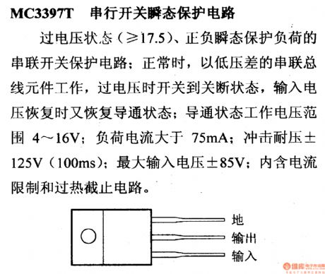
MC3397T serial switching transient protection circuit
Under the over-voltage condition (≥ 17.5), the positive and negative load protection serial switching transient protection circuit. During the normal operation, it works depending on low dropout serial component. The over-voltage leads to the off-state. When the input voltage has returned to lead state, the operating voltage under this state ranges with 4 ~ 16V. The load current is greater than 75mA and the impulse withstand voltage is ± 125V (100ms). Its maximum input voltage is ± 85V. Besides, it includes current limit and thermal cut-off circuit inside.
(View)
View full Circuit Diagram | Comments | Reading(688)
Voltage / frequency conversion circuit composed of AD654
Published:2011/7/10 22:23:00 Author:Lucas | Keyword: Voltage conversion , frequency conversion

In the circuit shown as Figure 1-1 (a), AD820 is a high-impedance input voltage / current conversion circuit. In the case of neglecting DC error, AD820's 2pA bias current can make input impedance be megohms magnitude. AD654 is voltage / current conversion circuit with a single supply voltage, whcih could make operating current be about 3mA. During the voltage conversion period, VTl output current I (T) could incent AD654 to control the output frequency f. In the circuit, C1 selects 1nF capacitor.
(View)
View full Circuit Diagram | Comments | Reading(657)
Regulator, DC-DC power supply monitor pin, main features MB3776 and other control circuit
Published:2011/7/8 0:32:00 Author:Lucas | Keyword: Regulator, power supply monitor, pin
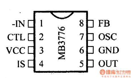
It shows the switching regulator control circuit. Its supply voltage ranges within 2.0 ~ 15V. The maximum standby current is 0.5μA and the work oscillation frequency ranges from 10 kHz to 500 kHz. And input (-IN side) voltage is limited within -0.3 ~ +10 V. Besides, the maximum collector current is 50mA. The double row DIP package is with power consumption of 550mA. Its operating temperature is between -30℃ to +75 ℃. With the dual push-pull output, it is possible to adjust internal drive circuit. And a resting time control circuit is included inside. The end of CTL can control the input and output of the power supply.
(View)
View full Circuit Diagram | Comments | Reading(818)
Regulator, DC-DC circuit, power supply monitor pin and main features MC147805 and other regulators
Published:2011/7/10 10:00:00 Author:Lucas | Keyword: Regulator, DC-DC circuit, power supply monitor, pin
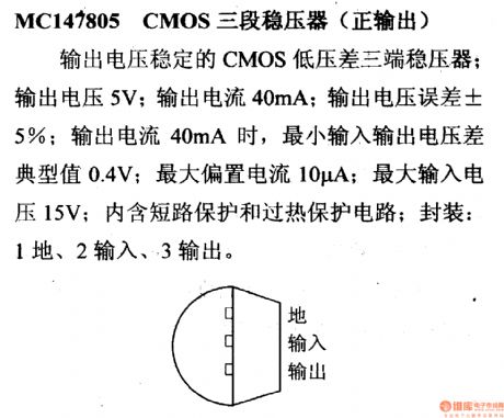
MC147805 CMOS’s three-stage regulator (positive output)
It is the CMOS low dropout three-terminal regulator with steady output voltage. Its output voltage is 5V and its output current is 40mA. The output voltage error is ± 5%. As the output current is 40mA, the minimum dropout voltage is typically 0.4V. The maximum bias current is 10μA and the maximum input voltage is 15V. It includes short protection circuit and thermal protection circuit inside. The package is with 1 ground, 2 input and 3 output.
(View)
View full Circuit Diagram | Comments | Reading(983)
Regulator, DC-DC power supply monitor pin, main features MC33065 and others control circuit
Published:2011/7/8 0:55:00 Author:Lucas | Keyword: Regulator, power supply monitor, pin
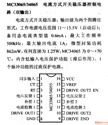
MC33065/34065 current mode switching regulator control circuit (dual output)
It is the current mode switching regulator whose output stages are formation of two totems. The regulator’s supply voltage ranges within 11 ~ 15.5V. And the standby state’s current is typically 0.6mA. The maximum working frequency is 500 kHz and the maximum output current is 1A. Besides, micro-encapsulated power consumption is 862mA. Its dual in-line is 1.25W. The MC34065 works within 0 ~ +70 ℃. Moreover, a low input voltage protection function device (hysteresis function) is placed inside, as well as a pulse overcurrent protection function circuit.
(View)
View full Circuit Diagram | Comments | Reading(689)
Regulator, DC-DC circuit, power supply monitor pin and main features MC3397T and other control circuits
Published:2011/7/10 10:42:00 Author:Lucas | Keyword: Regulator, DC-DC circuit, power supply monitor, pin
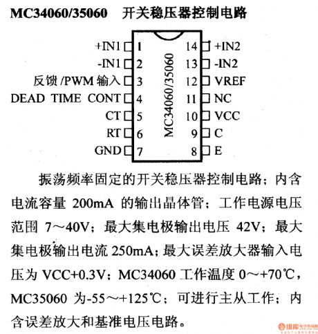
MC 34060/35060 switching regulator control circuit
It is switching regulator control circuit with the fixed oscillation frequency. It includes an output transistor with current capacity of 200mA. Its supply voltage ranges within 7 ~ 40V. The group large collector-level output voltage is 41V. And the largest collector-level output current is 250mA. The maximum input voltage of the error amplifier is VCC +0.4 V. The working temperature for 'MC34060 is from 0℃ to +70. That of the MC35060 is from- 55 ℃ to +125 ℃. It is available for master-slave working. Besides, it includes an error amplifier and reference voltage circuit.
(View)
View full Circuit Diagram | Comments | Reading(721)
TL496 switch regulator, main features and pin of DC-DC circuit and power supply monitor
Published:2011/7/10 2:04:00 Author:Lucas | Keyword: switch regulator, main features , pin , DC-DC circuit , power supply monitor
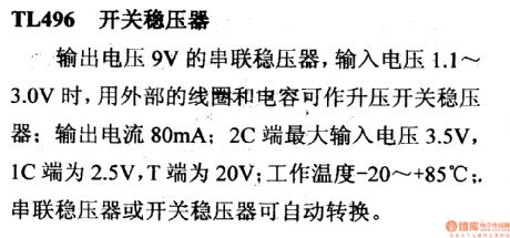
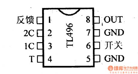
It is the series regulator with 9V output voltage, when input voltage is 1.1 ~ 3.0V, it uses an external coil and capacitoras step-up switching regulator; output current is 80mA; the maximum input voltage of 2C end is 3.5V; IC terminal is 2.5V, T end is 20V; Operating Temperature is -20 ~ +85 ℃; series regulator and switching regulator can be automatically converted.
(View)
View full Circuit Diagram | Comments | Reading(1746)
W1840 control circuit, main features and pin of DC-DC circuit and power supply monitor
Published:2011/7/10 2:32:00 Author:Lucas | Keyword: control circuit, main features , pin , DC-DC circuit , power supply monitor
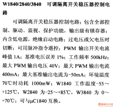
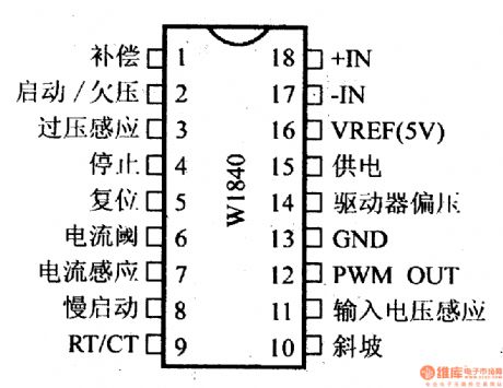
W1840/2840/3840 adjustable isolated switching regulator control circuit
It is the isolated switching regulator control circuit; it contains the functions of all the control, drive, monitor, protection, output stage latch; it contains low power, insulation start circuit; it cuts off when over voltage or under voltage; it is available in pulse command remote control; PWM Output switching current peak is 1A; reference voltage error is 1%; frequency is 500KHz; maximum PWM output voltage is 40V; maximum PWM output current is 400mA; maximum reference output current is -50mA; when ambient temperature is 70 ℃, the power is 1000mW; W1840 operating temperature is -55 ~ +125 ℃, W2840 is -25 ~ +85 ℃, W3840 is 0 ~ 70 ℃, and it is interchangeable with μC1840.
(View)
View full Circuit Diagram | Comments | Reading(514)
W4800 series of regulator, main features and pin of DC-DC circuit and power supply monitor
Published:2011/7/10 1:24:00 Author:Lucas | Keyword: regulator, main features , pin , DC-DC circuit , power supply monitor
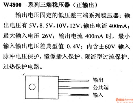
W4800 series of three-terminal regulator( positive output)
It is the three-terminal regulator with fixed output voltage; output voltage can be 5V, 8.5V, 10V, 12V; output current is 400MA; maximum input voltage is 26V; when output current is 400mA, the typically value of minimum dropout voltage is 0.4V; it contains ± 60V input pulse voltage protection, mirrored insert protection, current limiting type of overcurrent protection, overheat protection circuit.
(View)
View full Circuit Diagram | Comments | Reading(550)
W4920 series of regulator, main features and pin of DC-DC circuit and power supply monitor
Published:2011/7/10 1:41:00 Author:Lucas | Keyword: regulator, main features, pin , DC-DC circuit , power supply monitor
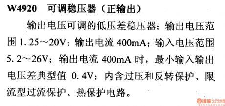
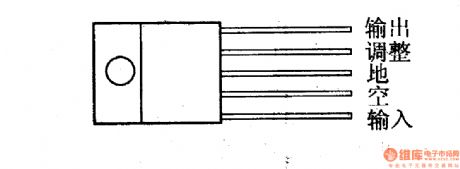
W4920adjustable regulator(positive output)
It is the three-terminal low dropout series of regulator with fixed output voltage; output voltage range is 1.25 ~ 20V; output current is 400mA; input voltage range is 5.2 ~ 26V; when output current is 400mA, the typical value of minimum dropout voltage is 0.4V; it includes overvoltage and reversal protection, current limiting type of overcurrent protection, thermal protection circuit.
(View)
View full Circuit Diagram | Comments | Reading(485)
W4960 switch regulator, main features and pin of DC-DC circuit and power supply monitor
Published:2011/7/10 1:58:00 Author:Lucas | Keyword: switch regulator, main features , pin , DC-DC circuit , power supply monitor
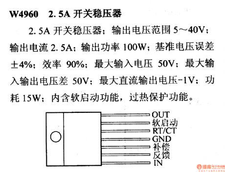
W4960 2.5A switch regulator
It is the 2.5A switching regulator; output voltage range is 5 ~ 40V; output current is 2.5A; output power is 100W; reference voltage error is ± 4%; efficiency is 90%; maximum input voltage is 50V;maximum difference between input and output voltage is 50V; the maximum DC output is -1V; power is 15W; it has the functions of soft start, thermal protection.
(View)
View full Circuit Diagram | Comments | Reading(549)
μA78G/79G series of regulator, main features and pin of DC-DC circuit and power supply monitor
Published:2011/7/9 8:38:00 Author:Lucas | Keyword: regulator , main features, pin , DC-DC circuit , power supply monitor
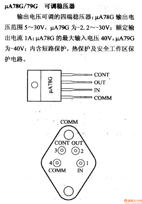
It is the four-terminal regulator with adjustable voltage; uA78G output voltage range is 5 ~ 30V, uA79G is -2.2 ~-30V; rated output current is 1A; the maximum input voltage of uA78G is 40V, uA79G is -40V; it includes short circuit protection, thermal protection and safe operating area protection circuit.
(View)
View full Circuit Diagram | Comments | Reading(1534)
The value circuit composed of DG201
Published:2011/7/6 8:47:00 Author:Lucas | Keyword: value circuit
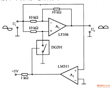
The circuit uses DG201 analog switch circuit and the zero-crossing comparator to control the polarity of the amplifier Al (in-phaseor inverting amplifier). When analog switch DG2O1 is off and the input signal is in positive half cycle, A2 output is in high level, and Al is a follower; when input signal is in negative half cycle, A2 output is in low level, then DGO1 is connected, and Al is equivalent to the inverting amplifier. In the circuit, A2 and DG2O1 is limited by the highest frequency, and the operating frequency is about lOkHz.
(View)
View full Circuit Diagram | Comments | Reading(1001)
TEX888H Communication Monolithic Micro-Computer Integrated Circuit Diagram
Published:2011/7/10 6:15:00 Author:Vicky | Keyword: Communication , Monolithic , Micro-Computer
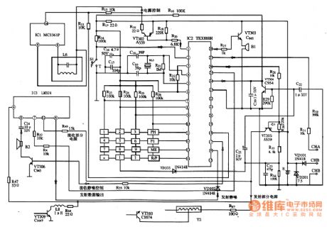
TEX888H is a communication monolithic micro-computer integrated circuit. It is usually used as mobile phone control circuit in cordless telephone.
Typical applied circuit diagram of mobile phone control which is composed of IC TEX888H is shown in picture 1.
Note: When dialing the number, failure in dialing is easy to happen to the mobile. Under such circumstance, check whether the keys are short-circuits or not first, whether the conductive rubber resistance becomes larger or not, and whether the inside mobile is affected with damp or not.
If password failure happens, you might emphasis on the check of the 18 pin of TEX888H and other exterior components. The possible reason of the malfunction can be judged by testing the dynamic or quiescent voltage of the pin. (View)
View full Circuit Diagram | Comments | Reading(3139)
Sound Control Twinkling Illuminations(3)
Published:2011/7/10 7:57:00 Author:Sue | Keyword: Sound Control, Twinkling, Illuminations
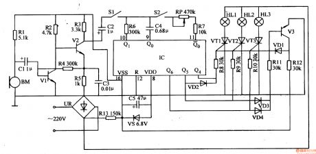
The 220v ac voltagewill provide the sound control circuit and IC with 6.8v direct current working voltage after it is rectificated by UR, limited and reduced by R13, stablized by VS, filtrated by C5.
S2,R6,R7,RP,C4 and IC's pin 9-11's inner circuits will compose oscillator circuit which will provide IC with count pulse. IC's Q4-Q6 terminals will output control voltage signals which will make VT1-VT3 connected by R8-R10,VD1-VD4,V3 in turn, or it will make two thyristors connected at the same time(or make 3 thyristors connected at the same time). HL1-HL3 will be illuminated in turn or two groups of illuminations will be illuminated at the same time(or 3 groups of illuminations will be illuminated at the same time). (View)
View full Circuit Diagram | Comments | Reading(613)
| Pages:1573/2234 At 2015611562156315641565156615671568156915701571157215731574157515761577157815791580Under 20 |
Circuit Categories
power supply circuit
Amplifier Circuit
Basic Circuit
LED and Light Circuit
Sensor Circuit
Signal Processing
Electrical Equipment Circuit
Control Circuit
Remote Control Circuit
A/D-D/A Converter Circuit
Audio Circuit
Measuring and Test Circuit
Communication Circuit
Computer-Related Circuit
555 Circuit
Automotive Circuit
Repairing Circuit