
Circuit Diagram
Index 1577
simple RCC power supply circuit with MOSFET synchronous rectification
Published:2011/7/9 4:18:00 Author:chopper | Keyword: simple, RCC power supply, MOSFET, synchronous rectification
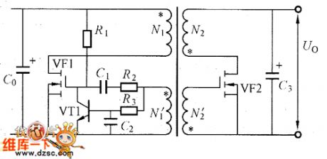
simple RCC power supply circuit with MOSFET synchronous rectification is shown as picture
(View)
View full Circuit Diagram | Comments | Reading(1737)
positive drive converter with synchronous rectification circuit
Published:2011/7/10 3:18:00 Author:chopper | Keyword: positive, drive converter, synchronous rectification
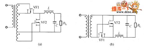
There are two current in the positive drive converter.One is the positive current through secondary winding when the primary side switching device is conductive,another is the current continued to circulate in the secondary side choke.Picture (a) is the instance of positive drive converter which adopts synchronous rectification.When the voltage of secondary winding is equal to the bias voltage of MOSFET grid,it can save some windings,just as shown in picture (b). (View)
View full Circuit Diagram | Comments | Reading(644)
TC-3330 Single-Chip Integrated Photoelectric Switch Driving Different Loads Application Circuit
Published:2011/7/9 6:49:00 Author:Robert | Keyword: Single-Chip, Integrated, Photoelectric Switch, Driving, Loads, Application
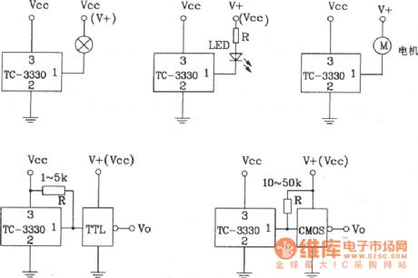
The picture shows the TC-3330 single-chip integrated photoelectric switch driving different loads application circuits.
The TC-3330 can also be used in many areas such as table code identification, tension sensing, optic fiber isolator, paper or object detection, counting, rotation speed measurement. the photoelectric coupler made with it (diode output type, triode output type, darlington type) has the excellent performance and high reliability and wide range of application. (View)
View full Circuit Diagram | Comments | Reading(822)
Half-wave synchronous rectification circuit with MOSFET
Published:2011/7/9 4:21:00 Author:chopper | Keyword: Half-wave, synchronous, rectification circuit, MOSFET
Half-wave synchronous rectification circuit with MOSFET is shown as picture
(View)
View full Circuit Diagram | Comments | Reading(838)
MOSFET drive circuit
Published:2011/7/9 3:41:00 Author:chopper | Keyword: MOSFET, drive circuit
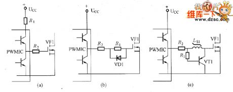
MOSFET drive circuit is shown as picture
(View)
View full Circuit Diagram | Comments | Reading(874)
CXA2089Q Multi-Function Electronic Switch Integrated Circuit
Published:2011/7/10 3:11:00 Author:Robert | Keyword: Multi-Function, Electronic, Switch, Integrated
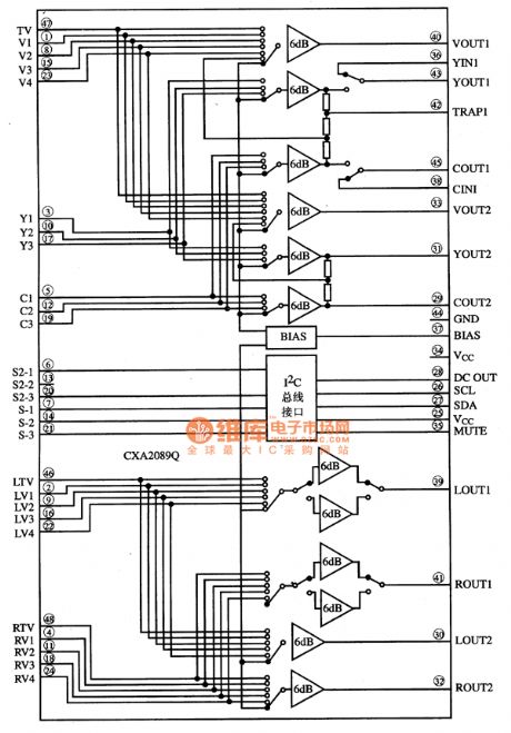
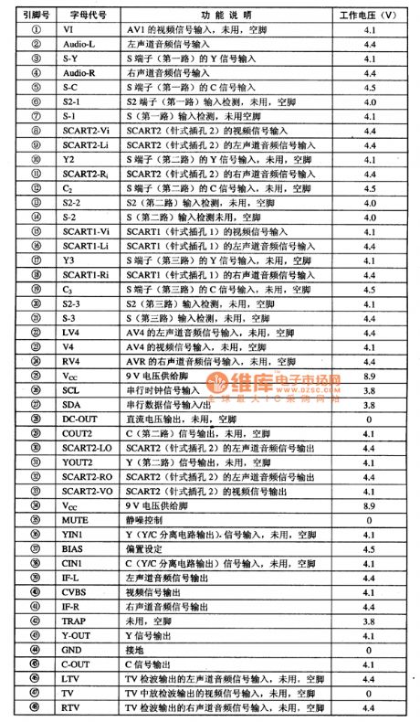
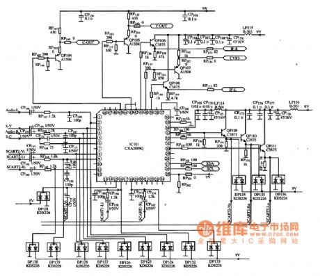
The CXA2089Q is a multi-function electronic switch IC produced by the Japanese Sony company which is widely used in domestic and imported plasma and other large-screen color TV sets, such as the LG series RF-02RA cassette mechanism and so on.
1.Its functional features.
The CXA2089Q IC has five groups composite video signal input, three groups Y/C signal input, two groups composite video signal output, 2 groups Y/C signal output, 5 groups L/R sound-channel audio signal input, 2 groups L/R sound-channel audio signal output, which support the S1 and 3-channel S2 protocol. It has internal Y/C hybrid circuit and wideband video amplifier (20MHz). Its audio squelch can be controlled from the external provided signal. The whole signal conversion is achieved under the I2C bus control.
The CXA2089A IC could not only achieve the internal and external video, internal and external double-sound-channel audio signal's conversion, but also can easily achieve the conversion between the external S-video port Y/C signal and internal Y/C signal separated from the Y/C separation circuit.
The CXA2089Q IC's internal circuit diagram is shown in picture 1.
The picture 1 shows the CXA2089Q IC's internal circuit diagram. (View)
View full Circuit Diagram | Comments | Reading(1661)
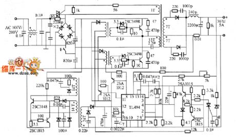
Switching power supply circuit with low-noise RCC mode
Published:2011/7/9 4:31:00 Author:chopper | Keyword: Switching, power supply, low-noise, RCC mode

Figure shows the grid drive circuit which uses the saturable reactor,switching power supply with low-noise RCC mode.Its output is 24V/4.5A, and it is as example of soft switching applications.
(View)
View full Circuit Diagram | Comments | Reading(3754)
AC RMS / DC converter circuit composed of AD533
Published:2011/7/6 8:01:00 Author:Lucas | Keyword: AC RMS converter, DC converter
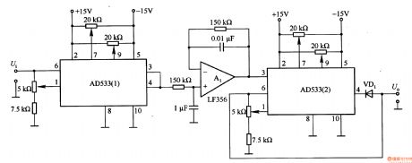
This is also circuit which could operate the multiplier AD533 and change AC RMS into the DC voltage. In the circuit, AD533 (1) makes the square operation on the input AC voltage instantaneous value, and its output is integrated by integrator Al, and square operated by AD533 (2), and AD533 (2)'s output is the the average value of input AC signal.
(View)
View full Circuit Diagram | Comments | Reading(2404)
Temperature-Sensitive Diode Application Circuit
Published:2011/7/10 2:47:00 Author:Robert | Keyword: Temperature-Sensitive Diode, Application
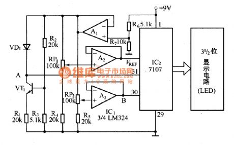
The circuit shown in the picture is the digital temperature meter circuit which uses temperature-sensitive diode as the temperature-measurement element. It is mainly made up of the A/D converter 7107, operational amplifier LM324, 3-digit LED display circuit and temperature-sensitive diode and so on. It features high accuracy, good stability, versatility, ease of use and so on. Its temperature measurement range is 0℃~100℃ with accuracy ±1℃.
The voltage follower, which is made up of the operational amplifier A1, supply power for the A/D converter integrated circuit IC2 and the temperature sampling circuit separately to reduce the interaction between them. The semiconductor transistor VT1 and R1, R2, R3 supply stable bias current for the temperature-sensitive diode VD1. (View)
View full Circuit Diagram | Comments | Reading(2195)
2ACM Type Magnetic-Sensitive Diode Shape Circuit
Published:2011/7/10 3:46:00 Author:Robert | Keyword: Magnetic, Diode, Shape
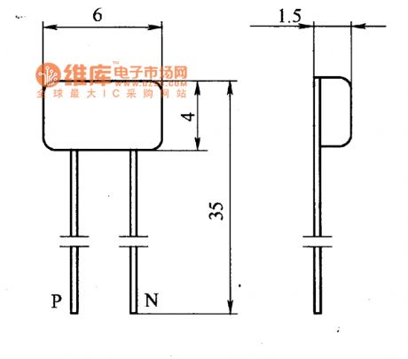
The picture shows the 2ACM type magnetic-sensitive diode shape circuit. (View)
View full Circuit Diagram | Comments | Reading(845)
DPTV-3D6730 Image Processing Integrated Circuit
Published:2011/7/9 22:59:00 Author:Robert | Keyword: Image, Processing, Integrated

The DPTV-3D673 is a image processing IC which is used in the super-large screed rear projection color TV sets, such as the Changhong HP series Precision Vision King and so on.
1.Its functional features.
The DPTV-3D6730 IC's internal circuit can be used to complete the image signal's A/D (analog/digital) conversion, NTSC/SECAM modulation and decoding, scanning frequency and format conversion, 14D dynamic picture quality enhancement, digital/analog (D/A) conversion and so on.
(1)Its decoding circuit.
The decoding circuit has a 3D comb filter controlled by the program, which can support PAL/NTSC/SECAM formats and isolate the Y/C signals. The color edge enhancement circuit can improve the color transient characteristics.
(2)Screen diaplay modes.
The screen display modes mainly have: picture-out-picture display mode, picture-in-picture display mode, panorama display mode. It supports 16:9 and 4:3 screen ratio and other modes. (View)
View full Circuit Diagram | Comments | Reading(644)
AC RMS / DC converter circuit composed of AD536J
Published:2011/7/6 7:52:00 Author:Lucas | Keyword: AC RMS converter , DC converter
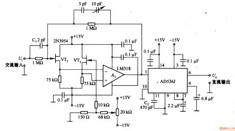
This is an operational AC RMS / DC conversion circuit, which could change AC RMS into the operation of DC voltage. AD536J input impedance is lower with only about 16kΩ, so the application should access the input buffer. In the figure, Al (LM318) is the buffer, the input impedance can be increased to lMΩ. Cl is the frequency compensation capacitor, and C2 is high-frequency compensation capacitor, which can change its capacity to improve the frequency characteristics.
(View)
View full Circuit Diagram | Comments | Reading(3661)
D2025 Dual-Sound-Channel Audio Power Amplification Integrated Circuit
Published:2011/7/9 7:35:00 Author:Robert | Keyword: Dual-Sound-Channel, Audio, Power, Amplification, Integrated
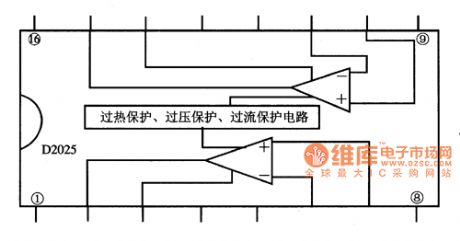
The D2025 is a dual-sound-channel audio power amplification IC which is widely used in the computer active speakers and other equipments.
1.Its functional features.
The D2025 IC's internal part is mainly made up of two-channel power amplifier with the same function and over-heat protection circuit, over-voltage protection circuit, over-current protection circuit and other circuits. Its internal circuit diagram is shown in picture 1.
The picture 1 shows the D2025 IC's internal circuit diagram.
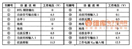
2.Its pin's function and data.
The D2025 IC uses 16-pin dual inline package and its pin's function and data is listed in table 1.
The table 1 shows the D2025 IC's pin's function and data.
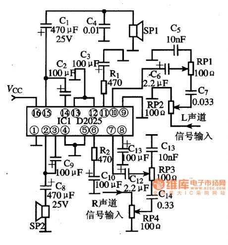
3.Typical application circuit.
The dual-sound-channel power amplification typical application circuit composed of D2025 IC is shown in picture 2.
The picture 2 shows the D2025 IC's typical application circuit. (View)
View full Circuit Diagram | Comments | Reading(5592)
typical circuit of voltage resonant converter
Published:2011/7/10 2:55:00 Author:chopper | Keyword: typical, voltage, resonant converter
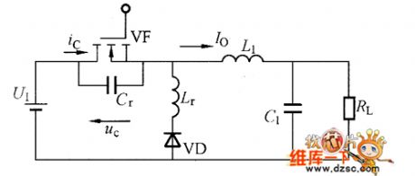
Voltage resonant circuit and current resonant circuit are in dual relationship.As to voltage resonant circuit,voltage uc(t) of switch ends is converted into sine wave voltage through resonant circuit when the switch tube is close,and the voltage is zero when switch is on/off,thus to decrease the consumption and surge.This is the so-called zero-voltage switch.
(View)
View full Circuit Diagram | Comments | Reading(626)
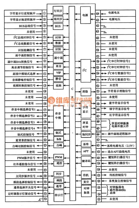
CXP750096-012Q Single-Chip Micro-Computer Integrated Circuit
Published:2011/7/9 7:47:00 Author:Robert | Keyword: Single-Chip, Micro-Computer, Integrated
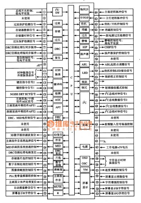
The CXP750096-012Q is a single-chip micro-computer IC produced by the Japanese Sony company. It is widely used in the digital color TV sets.
1.Its functional features.
The CXP750096-012Q IC's internal part is mainly made up of central processing unit (CPU), clock oscillation circuit, decoding circuit, I2C bus control circuit, screen display character generating and processing circuit, picture-in-picture control circuit, starting control circuit, and other some control and auxiliary function circuits and so on. Its internal circuit diagram is shown in picture 1.
The picture 1 shows the CXP750096-012Q IC's internal circuit diagram and pin's function and signal flowing.
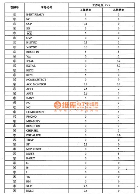
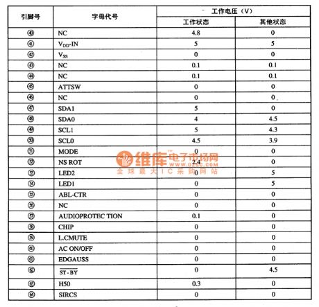
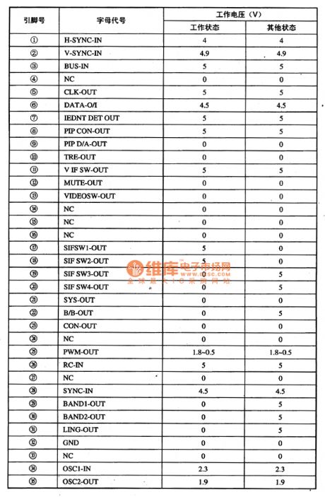
2.Its pin's letter code and data.
The CXP750096-012Q IC uses 64-pin dual package and its pin's letter code and data is listed in the table 1.
The table 1 shows the CXP750096-012Q IC's pin's letter and data. (View)
View full Circuit Diagram | Comments | Reading(628)
AC / DC conversion circuit composed of LM3O1A
Published:2011/7/6 19:13:00 Author:Lucas | Keyword: AC conversion, DC conversion
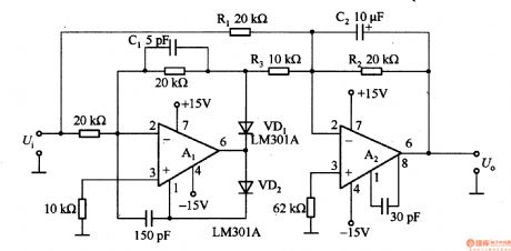
Operational amplifier Al is connected in series in the feedback circuit to be used as the inverting amplifier, for negative input signal, VDl is stopped and not related to circuit, so Al output is 0V. A2 works as the gain of -R2Ui/Rl according to the resistance of Rl, R2. For positive input signals, A2 adds the signal from R3 and Rl. If R3 = Rl / 2, the U. = UiR2/Rl. In order to get the output voltage which is equal to the average of the input voltage, then C2 and R2 provide low-pass filter characteristics for A2.
(View)
View full Circuit Diagram | Comments | Reading(1100)
CXP85332-108 Single-Chip Micro-Computer Integrated Circuit
Published:2011/7/9 8:05:00 Author:Robert | Keyword: Single-Chip, Micro-Computer, Integrated

The CXP85332-108 is a single-chip micro-computer IC produced by the Japanese Sony company. It is widely used in the Sony series large-screen digital color TV sets.
1.Its functional features.
The CXP85332-108 IC's internal part is mainly made up of central processing unit (CPU), clock oscillation circuit, reset control circuit, remote-control command signal processing circuit, I2C bus control circuit, key command signal decoding circuit, standby/starting control circuit, picture-in-picture control circuit, screen display character generating and processing circuit and other some control and auxiliary function circuits and so on. Its internal circuit diagram and pin's function and signal flowing is shown in picture 1.
The picture 1 shows the CXP85332-108 IC's internal circuit diagram and pin's function and signal flowing.
2.Its pin's letter code and data.
The CXP85332-108 IC uses 64-pin dual package and its pin's letter code and data is listed in the table 1.
The table 1 shows the CXP85332-108 IC's pin's letter and data. (View)
View full Circuit Diagram | Comments | Reading(909)
Half-bridge practical switching power supply circuit
Published:2011/7/10 2:39:00 Author:chopper | Keyword: Half-bridge, practical, switching, power supply circuit
Half-bridge practical switching power supply circuitis shown as picture
(View)
View full Circuit Diagram | Comments | Reading(4139)
RCC practical switching regulator circuit
Published:2011/7/10 3:06:00 Author:chopper | Keyword: RCC, practical, switching regulator circuit
RCC practical switching regulator circuit is shown as picture
(View)
View full Circuit Diagram | Comments | Reading(1641)
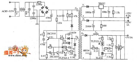
CXP80420-1391 Single-Chip Micro-Computer Integrated Circuit
Published:2011/7/9 8:13:00 Author:Robert | Keyword: Single-Chip, Micro-Computer, Integrated
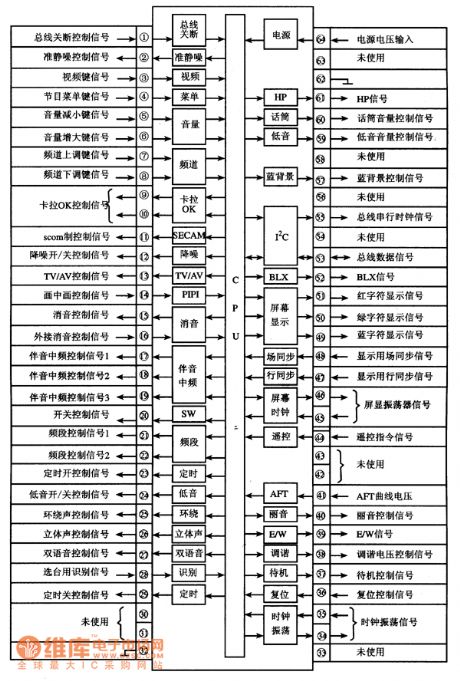
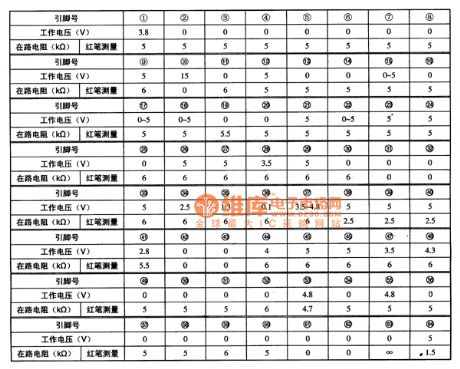
The CXP80420-1391 is a single-chip micro-computer IC which is widely used in the Japanese Sony series large-screen digital color TV sets.
1.Its functional features.
The CXP85332-108 IC's internal part is mainly made up of central processing unit (CPU), clock oscillation circuit, reset control circuit, I2C bus control circuit, screen display character generating and processing circuit and other some control and auxiliary function circuits and so on. Its internal circuit diagram and pin's function and signal flowing is shown in picture 1.
The picture 1 shows the CXP80420-1391 IC's internal circuit diagram and pin's function and signal flowing.
2.Its pin's letter code and data.
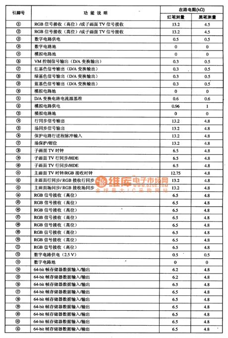
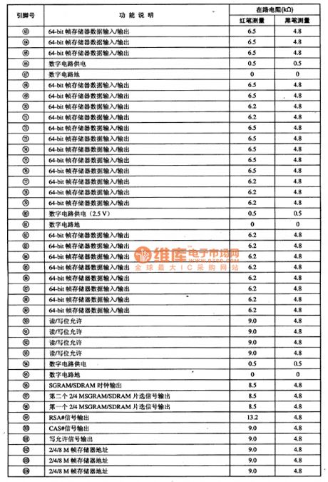
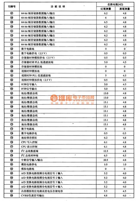
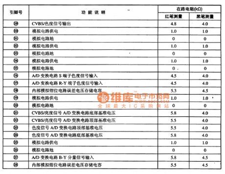
The CXP80420-1391 IC uses 64-pin dual package. Its pin's function is shown in the picture 1 and its working parameters are listed in the table 1.
The table 1 shows the CXP85332-108 IC's working parameters. (View)
View full Circuit Diagram | Comments | Reading(973)
| Pages:1577/2234 At 2015611562156315641565156615671568156915701571157215731574157515761577157815791580Under 20 |
Circuit Categories
power supply circuit
Amplifier Circuit
Basic Circuit
LED and Light Circuit
Sensor Circuit
Signal Processing
Electrical Equipment Circuit
Control Circuit
Remote Control Circuit
A/D-D/A Converter Circuit
Audio Circuit
Measuring and Test Circuit
Communication Circuit
Computer-Related Circuit
555 Circuit
Automotive Circuit
Repairing Circuit