
Circuit Diagram
Index 1572
MAX16802 Typical Appliction Circuit
Published:2011/6/28 0:40:00 Author:Michel | Keyword: Typical, Appliction, Circuit
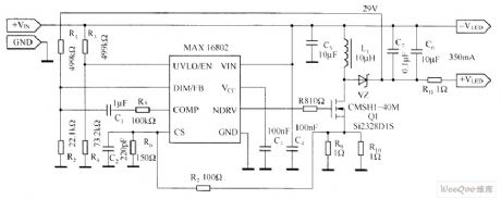
MAX16802 Typical Circuit is shown as above.Inspection flow resistance is compsoed of R9 and R10 in parallel form and voltage detection dividing resistor consists of R6 and R7.The MAX16802 current limit threshold is 291 mV, so we choose R9, R10, R6, and R7 can meet the calculated inductance peak current. Becuase of parasitic effect in the circuit,the resistance R7 value need proper adjustment to get the expecting current.
Picture:MAX16802 Typical Appliction Circuit (View)
View full Circuit Diagram | Comments | Reading(972)
Enhanced RS-485 interface with isolation circuit
Published:2011/7/7 7:21:00 Author:Fiona | Keyword: Enhanced interface, with isolation
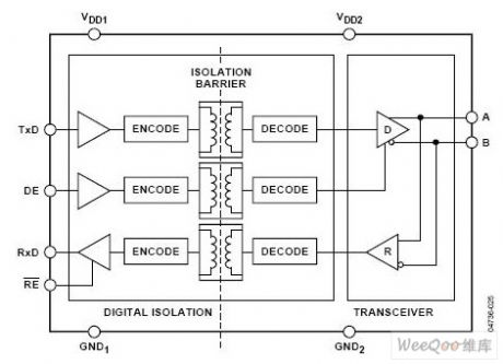
ADM2483 is enhanced RS-485 transceiver with isolation, the internal block diagram is shown as Figure 1,which includes a three-channel isolator,a differential drive with three-state output and a differential receiver with three-state input.The receiver with 1 / 8 unit load inputs impedance that allows more than 256 transceivers to access bus, the highest transfer rate is 500Kbps. Logical end is compatible with 3V/5V power supply, the bus terminal has 5V power supply.Compared with other RS-485 interface chips,ADM2483 integrates the magnetic isolation technology,it only requires an external DC/DC power supply.
(View)
View full Circuit Diagram | Comments | Reading(2213)
The CAN total line interface circuit of vortex flowmeter
Published:2011/7/8 3:25:00 Author:Fiona | Keyword: The CAN total line interface, vortex flowmeter
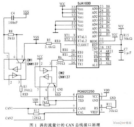
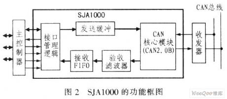
CAN total line is a serial data communication protocol,in CAN total line communication interface integrates the CAN protocol's the physical layer and data link layer,it can accomplish the process of framing to the communication data.The author is regard SJA1000 as Flowmeter's CAN controller,it is connected to the I/O of CPU(SCM) immediately so that it composes CAN total line of PCA82C250.This contruction is very easy to achieve sending and receiving information of CAN network nodes,thus achieves on-site control.SJA1000's AD0~AD7 is connected to MSP420F149's P0,INT is connectedto P1.0,/CS is connectedto P1.1,/RD is connected to P1.2,/WR is connected to P1.3,ALE is connected to P1.4,after being respectively connected through two high-speed optocoupler CNW137 and PCA82C250,TX0 and RX0 of SJA1000 are connected to the CAN total line.
(View)
View full Circuit Diagram | Comments | Reading(1345)
The crossbar user extension outside metering device circuit
Published:2011/7/7 7:22:00 Author:Fiona | Keyword: The crossbar user, extension outside metering device
The crossbar user extension outside metering device circuit is shown as above,this device is suitable for HJ-905, HJ-906-type extension outside metering device that the the crossbar user switchboard. The metering device has a easy circuit, low cost and easy maintenance features.As the counting device is for each extension units,for convenience of copy times,it equips with 4-digit electromagnetic counter,it's eye-catching visual. The metering device is composed of pulse shaping,pulse string of gap detection, the first 0 discrimination, pulse string of records, timing and counting circuit and other circuit.
(View)
View full Circuit Diagram | Comments | Reading(1066)
SCM and SJA1000 CAN controller interface circuit
Published:2011/7/8 3:30:00 Author:Fiona | Keyword: controller interface
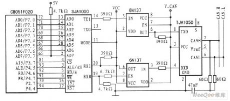
The picture shows the C8051F020 SCM and hardware connection circuit principle of SJA1000 controller.SJA1000 takes up 0x8000-0x80FF external RAM space.When SCM visits the above space,the chip select signal will select SJA1000. C8051F020 has high and low two external memory interfaces. Therefore,the AD0-AD7 of SJA1000 is connected to high port P7 of C8051F020, CS is connected to the chip select signal of external memory which the base address is 0x8000.When C8051F020 visits 0x8000-0x80FF,CPU can execute the corresponding read / write operations to SJA1000.RD,WR and ALE of SJA1000 are connected to corresponding pin of C8051F020,INT is connected to the INT0 pin of C8051F020,so that C8051F020 can visit SJA1000 through interrupt mode.
(View)
View full Circuit Diagram | Comments | Reading(3596)
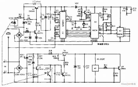
MC34011 voltage-stabilizing circuit
Published:2011/7/8 3:44:00 Author:Fiona | Keyword: voltage-stabilizing
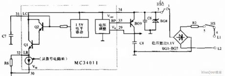
MC34011 voltage-stabilizing circuit is shown as above,NC34011 voltage-stabilizing circuit consists of a part of this chip,the external whole bridge,voltage regulator BG8 and other circuit. Its function is providing stable 1.1V DC voltage for the MC34011 working,the stable DC voltage is sent to 3,4 pins of MC34011 by the emitter of BG9.
(View)
View full Circuit Diagram | Comments | Reading(1233)
MC34011 ringing circuit
Published:2011/7/8 3:57:00 Author:Fiona | Keyword: ringing
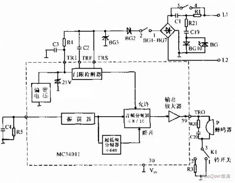
MC34011 ringing circuit is shown as above,the carrier ring signal sent by L1,L2 is sent into the ringing signal processing circuit of MC3401 after the bridge rectifying(threshold detection,comparison frequency division,output amplification, etc.).The ring signal is sent out from 39 pin to the buzzer.The loudness of the buzzer is controlled by K1 switch,when K1 is set at 1 ,the buzzer rings;when K1 is set at 2 ,the buzzer is light.
(View)
View full Circuit Diagram | Comments | Reading(838)
TEA1062 talking circuit
Published:2011/7/8 4:07:00 Author:Fiona | Keyword: talking
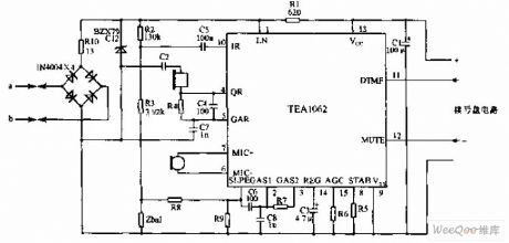
TEA1062 talking circuit is shown as above,TEA1062 is bipolar integrated circuit produced by Philips company,it can complete the voice access,the line interface and the dial interface functions,dialing and talking use electronic conversion,low call uses electronic conversion,there is as low as 1.6V DC line voltage to adapt to many parallel machines.The figure is typical application in the phone.
(View)
View full Circuit Diagram | Comments | Reading(4545)
series attenuation test circuit
Published:2011/7/8 4:13:00 Author:Fiona | Keyword: attenuation test
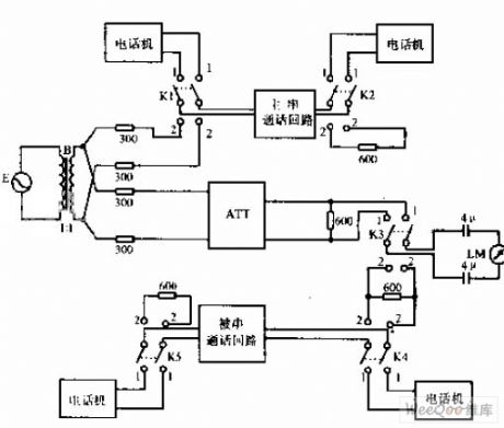
Compared with the transmission attenuation measurement circuit,series attenuation test circuit adds two pole-throw switch K4,K5.
(View)
View full Circuit Diagram | Comments | Reading(810)
Single audio decoding circuit
Published:2011/7/8 4:26:00 Author:Fiona | Keyword: Single audio decoding
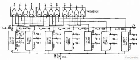
Single audio decoding circuit is shown as above,the figure is the used for dual tone multiple frequency(DTMF) demoder circuit.DTMF modulating signal sent from external line leads to the single narrowband filter which is composed of integrated circuit LM567 and the seven center frequencies are 697 ~ 1447Hz,then it is paired sent into nand gate and outputs corresponding 1,2, ... , 9,0 and other numbers.
(View)
View full Circuit Diagram | Comments | Reading(990)
Telephone anti-theft trick lock circuit
Published:2011/7/8 10:36:00 Author:Fiona | Keyword: anti-theft trick lock
Telephone anti-theft trick lock circuit is shown as above, this lock's specific functions as follows: 1.1~4 any limited prefix numbers, such as 0 , 173 , 9688 , can lock 1000 groups. 2.4 * password,confidentiality is strong.3.it can change the password and limited number at any time.4.* it delays about 6S to automatically shut after call to prevent free call on limited number. 5 Setting the password and limited number are operated on telephone.6.When the outside line is parallel operation theft,it makes a alarm sound to disturb the theft phone, while the red light is bright.7.The green light is bright when the users calling,it says the line is busy. Circuit is divided into limited local dial-up and parallel operation thief dozen two completely independent parts.
(View)
View full Circuit Diagram | Comments | Reading(779)
Telephone electronic ringer circuit
Published:2011/7/8 11:24:00 Author:Fiona | Keyword: electronic ringer
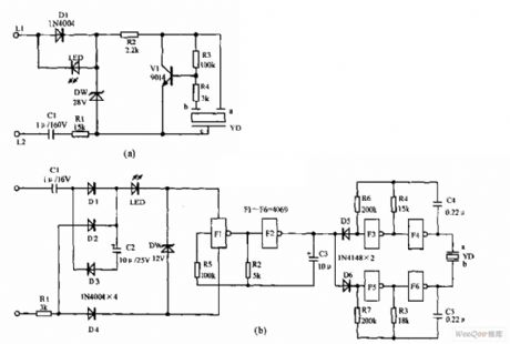
Telephone electronic ringer circuit is shown as above,Figure (a) is the electronic ring circuit with an NPN transistor V1 (choose 9014 or 3DG12) as the core, sound devices YD is also feedback devices composed of the feedback pole and the buzzer equipped with the help of the sound chamber. L1, L2 connect to circuit line;C1 and R1 have limiting and reducting voltage effects; R2 is the isolation resistor.D1 is the commutation diode.DW is the clamper tube. Figure (b) is the electronic ringing circuit with A general CMOS integrated block CD4069(or 4069, MC4069, TC4069)as the core design.
(View)
View full Circuit Diagram | Comments | Reading(2638)
Telephone burglar alarm circuit
Published:2011/7/9 9:53:00 Author:Fiona | Keyword: burglar alarm
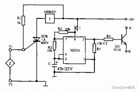
Telephone burglar alarm circuit is shown as above,it is formed by the SCR,relay,NE555 and peripheral components. When the sensor Z is connected, the whole machine is in waiting state,the circuit works. A, B are respectively connected to telephone handfree knob which is stored at pulse dial-up and has the hands free function and the joint of the storage number keys.When the sensor Z is off due to happen stolen situation,the circuit works,A and B are connected,it is equal to off-hook and sending out the storage alarm number (such as 110 or your local phone number).
(View)
View full Circuit Diagram | Comments | Reading(1048)
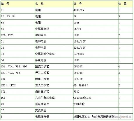
Lost Reminder
Published:2011/7/10 22:12:00 Author:Felicity | Keyword: Lost Reminder
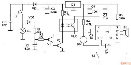
Work of the circuit
The circuit consists of power circuit, trigger control circuit and voice circuits. (It is showed in picture 7-116.)
Power circuit consists of battery GB, diode VDl, filter capacitor C2, C4, C5 and the voltage regulator integrated circuit ICl.
The trigger control circuit consists of door switch SI, door light EL, the diode VD2, resistors Rl-R3, capacitor Cl, transistors Vl, V2, and pomegranate combined optical device VLC.
Voice circuit consists of microphone BM, recording switch S2, voice integrated circuit IC2, capacitor C3, C6, resistors R4, R5 and speaker BL. (View)
View full Circuit Diagram | Comments | Reading(813)
Telephone diacritical transponder circuit
Published:2011/7/9 2:55:00 Author:Fiona | Keyword: diacritical transponder
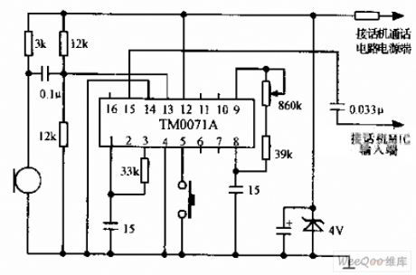
Telephone diacritical transponder circuit is shown as above,the diacritical transponder increases diacritical speaker function for the telephone and keeps secret for identity of the person who answers the phone.Diacritical integrated circuit TM0071A (or KTS00T1A) is New single piece of large-scale speech processing integrated circuit and dual in-line 16-pin package,the voltage range is 3 ~ 5V, the power supply can be obtained after the telephone power supply maintains the voltage.When installing,it removes the transmitter MIC of theoriginal telephone,connects the MIC input terminal of the output connection phone and power supply side to telephone power supply,all components can be mounted on a small circuit board.The circuit board can be put in the phone's leisure place.Function conversion can use a micro switch which is fixed on the phone shell.
(View)
View full Circuit Diagram | Comments | Reading(933)
Telphone convenient lamp circuit
Published:2011/7/9 2:31:00 Author:Fiona | Keyword: convenient lamp
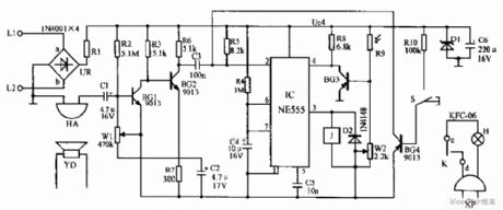
Telephone convenient lamp circuit is shown as above,S is the tact switch connected with microphone key,it is off at ordinary times, it is connected in off-hook status.HA is piezoelectric ceramic chip which is pasted in the speaker YD,L1 and L2 are the telephone lines.When it has no ringing signal or it isn't in off-hook state,3 terminal of NE555 is low potential,relay J does not work,and when it has a ringing signal or it is in off-hook state, J is conducted to make K close and H light.it is thus clear that the convenient lamp provides timely lighting when you receive and make a call at night.
(View)
View full Circuit Diagram | Comments | Reading(625)
Single metal chip touch switch circuit
Published:2011/7/9 1:57:00 Author:Fiona | Keyword: Single metal chip
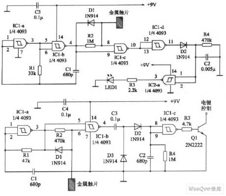
The circuit shown in the figure only uses a touch metal chip,the circuit uses two forty-two input terminals(internal has four identical, with two input terminals) schmitt trigger 4093(such as CD4093,TC4093 etc.).Usually the output terminal's 3 pin of IC2-a is low,light-emitting diode LED1 can not shine,when touching metal chip, the output terminal changes into high level to make the LED1 turn and light.
(View)
View full Circuit Diagram | Comments | Reading(2158)
Undervoltage,overvoltage protection alarm circuit
Published:2011/7/9 2:07:00 Author:Fiona | Keyword: undervoltage,overvoltage protection, alarm
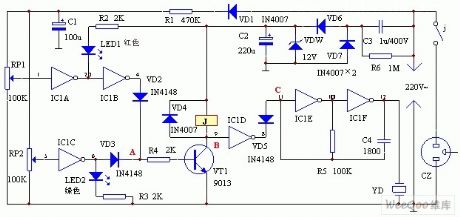
Work principle
Circuit is shown as above.Mains voltage reduces voltage by C3,maintains voltage by DW,VD6,VD7,C2 rectifier filter output maintaining DC voltage supply circuit.Another path is rectified by VD1,reduced voltage by R1 and filtered by C1, the voltage about 12V produced in RP1、RP2 detects the input signal of the mains voltage change.Door IC1A,IC1B form the overvoltage detection circuit, IC1C is undervoltage detection,IC1D is switch,IC1E,IC1F,piezoelectric ceramicchip YD and other components form the audio pulse oscillator. Transistor VT,relay J and other components form the protection movement circuit.Red LED1 is for mains overvoltage indication,the green LED2 is for mains voltage undervoltage indication.
(View)
View full Circuit Diagram | Comments | Reading(3588)
In-phase audio amplifier circuit
Published:2011/7/9 1:07:00 Author:Fiona | Keyword: In-phase, audio amplifier
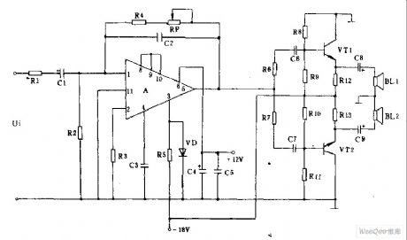
The Working principle is shown as above:input audio weak signal is amplified by amplifier A's 1 pin after capacitance cl coupling.The signal putout by @ pin and two parallel symmetrical, balance of power amplifier transistor VTl,VT2 emitters are in-phase output.In the circuit, c2, R4, RP form the negative feedback circuit to improve the stability of the output waveform.c3 is compensatory high frequency capacitor. C4, c5 are power supply AC component filter capacitors.Resistor R8 ~ Rlj are the bias resistors of transistor vTl,vT2. Low frequency end stand or fall depends on the capacity size of the output capacitors C8, c9 at the output end,meanwhile,it plays the every straight role,adjust potentiometer RP can adjustable gain up to 10dB or more. (View)
View full Circuit Diagram | Comments | Reading(1322)
Phone number coded lock circuit
Published:2011/7/9 0:38:00 Author:Fiona | Keyword: number coded lock
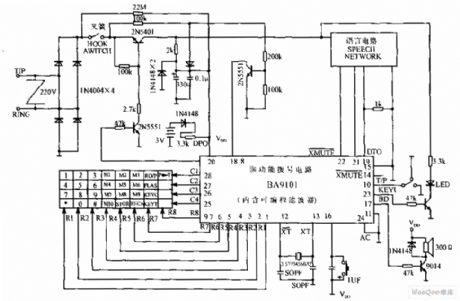
Phone number coded lock circuit is shown as above,this picture is the specific application circuit of digital password integrated blocks BA9101,it is composed of keyboard,multi-functional dial-up integrated network circuit,peripheral control circuit and so on.This coded lock has a major, minor secondary control,it is suitable for three kinds of use levels and can respectively control according parameters.Keeping password and parameters is supplied by the lithium battery,it is not lost in five years.
(View)
View full Circuit Diagram | Comments | Reading(1113)
| Pages:1572/2234 At 2015611562156315641565156615671568156915701571157215731574157515761577157815791580Under 20 |
Circuit Categories
power supply circuit
Amplifier Circuit
Basic Circuit
LED and Light Circuit
Sensor Circuit
Signal Processing
Electrical Equipment Circuit
Control Circuit
Remote Control Circuit
A/D-D/A Converter Circuit
Audio Circuit
Measuring and Test Circuit
Communication Circuit
Computer-Related Circuit
555 Circuit
Automotive Circuit
Repairing Circuit