
Circuit Diagram
Index 1873
The oil spray control system circuit of 200GLi AFE petrol engine
Published:2011/5/16 8:47:00 Author:Borg | Keyword: oil spray control system, Santana
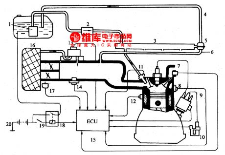
Figure 1 The electric controlled oil spray system of Santana 200GLi AFE petrol engine
1-power petrol pump; 2-petrol filter; 3-general fuel distributor; 4-oil return tube; 5-oil pressure adjuster; 6-vacuum tube; 7-oxygen sensor; 8-coolant temperature sensor; 9-electricity distributor; 10-igniting coil; 11-oil sprayer; 12-explosive sensor; 13-idling speed; 14-admission control valve; 15-electric control unit(computer); 16-air filter; 17-throttle position sensor; 18-petrol relay; 19-igniting switch; 20-battery (View)
View full Circuit Diagram | Comments | Reading(2156)
BA3304F-the integrated circuit of 2-channel audio preamplifiers
Published:2011/5/15 5:38:00 Author:Borg | Keyword: integrated circuit, 2-channel, audio preamplifiers
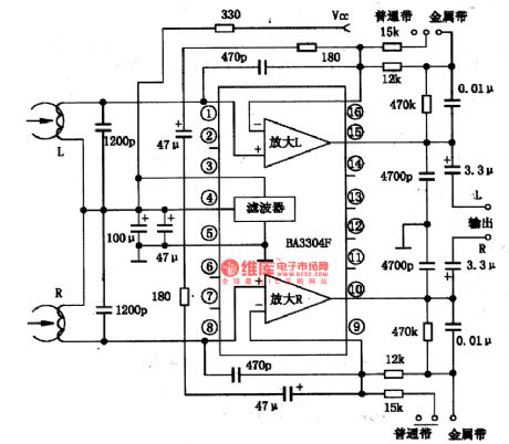

BA3304F is an integrated circuit of 2-channel audio preamplifiers produced by Toyo Power Tool Corp., Japan, which is used in miniature stereo players.1.the internal circuit and pin functions of BA3304FBA3304F consists of two teams of sub-circuits of preamplifiers and frequecy compensation, and filters, etc. Figure 1 is the internal circuit and typical application circuit. And the IC is in flat 16-lead dual line packages, whose pin functions and data are listed in Table 1.
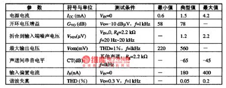
2.main parameters of BA3304F
(View)
View full Circuit Diagram | Comments | Reading(971)
The electric spray system control circuit of Santana 200GLi AFE petrol engine(2)
Published:2011/5/16 8:08:00 Author:Borg | Keyword: electric spray system, control circuit, Santana
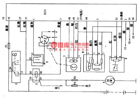
The electric spray system control circuit of Santana 200GLi AFE petrol engine(2)
(View)
View full Circuit Diagram | Comments | Reading(873)
The gasoline injection engine circuit of Santana 2000GLi
Published:2011/5/16 20:10:00 Author:Borg | Keyword: gasoline injection engine, Santana
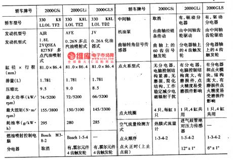
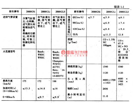

Since 1985, the Santana LX,GX and GX5 produced by Shanghai Volkswagon Corp. by using German Volkswagon technology have taken 1/2 of Chinese car market.Several Santana 2000 comparison
Because there are many types and specifications of Santana manufactured by the car factories in German and other countries, the circuits are different. Therefore, when inputting the manufactureing technology and developing new cars, Shanhai branch has done some modification and supplement considering the state of our country.
(View)
View full Circuit Diagram | Comments | Reading(939)
The igniting distributor circuit of Santana 2000GLi
Published:2011/5/16 7:12:00 Author:Borg | Keyword: igniting distributor, Santana
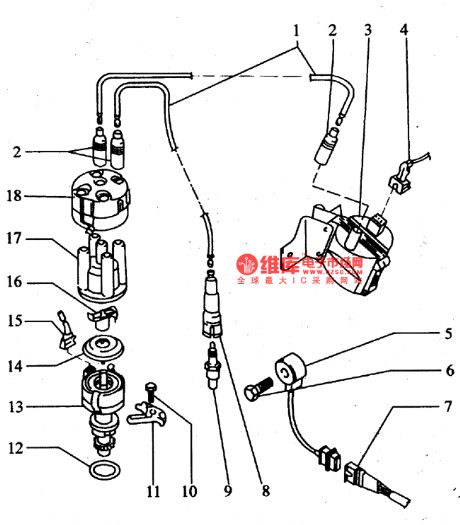
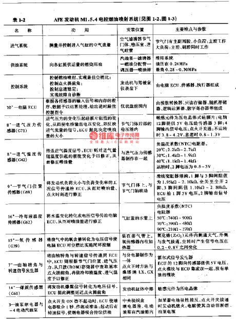
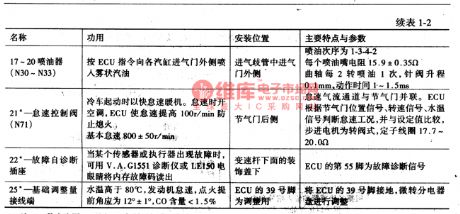
Figure 1 The igniting distributor circuit of Santana 2000GLi1-high voltage wire; 2-anti-noise plug(0·9-lkΩ); 3-igniting coil; 4-igniting coil connector; 5-explosive sensor(C6l is on the cylinder of engine); 6-screw; 7-explosive sensor plug; 8-spark plug(4.5-5.5kΩ); 9-spark piston; 10-screw of electricity distributor board(25Nm); 11-electricity distributor board; 12-O-shape coil; 13-igniting electricity with Hall sensor(g40); 14-shield; 15-Hall sensor plug; 16-distributor rotor(model No.Rl,1.lkΩ); 17-electricity distributor; 18-shielding case
(View)
View full Circuit Diagram | Comments | Reading(601)
Operational amplifier universal CNC offset adjustment circuit diagram
Published:2011/5/12 4:22:00 Author:Rebekka | Keyword: Operational amplifier, universal CNC , offset adjustment
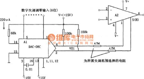
Figure shows the operational amplifier universal CNC offset adjustment circuit. The imbalance change uses digital control. The integrated chip DAC-08C is used as the six D / A converter. ②, ④ are output pins, they externally connect with two l00kΩ resistors. These 2 resistor is equivalent to load resistance. It generates output voltage Vo1. The output voltage Vo1. It passes the two 4.7MΩ large resistors and turns to the A2 offset adjusting current. The two 4.7MΩ large resistors are set by the range of disorders. The circuit is useful to the big circuit system. Because virtually any offset voltage can be stored in the memory, you can add it to the the amplifier when it is necessary. (View)
View full Circuit Diagram | Comments | Reading(916)
Optional frequency coefficient time delay circuit diagram
Published:2011/5/13 4:05:00 Author:Rebekka | Keyword: Optional frequency coefficient, time delay
Optional frequency coefficient time delay circuit diagram is shown as above. The circuit is composed of two 7-bit binary serial counters CC4024, controlled pulse source (gate 1, 2 components) and input, output control circuit. (View)
View full Circuit Diagram | Comments | Reading(771)
Simple differential amplifier circuit diagram composed of μA709
Published:2011/5/13 3:06:00 Author:Rebekka | Keyword: Simple differential amplifier
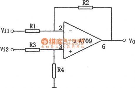
Simple differential amplifier circuit is shown as above. Two input signals Vi1 and Vi2 are added to the input terminal after passing the R1 and R3, R4 divide voltage circuit. Vi1 is added to the inverting input of the op amp, Vi2 is added to the same input terminal. The relationship of the output voltage Vo and Vi1, Vi2 are shown as above.
The output voltage is R2/R1 times of the difference between the two signals. It can get a different output voltage by proper selection of the ratio of R2/R1. (View)
View full Circuit Diagram | Comments | Reading(1646)
μA741 dual power universal single op amp circuit diagram
Published:2011/5/13 2:47:00 Author:Rebekka | Keyword: dual power, universal single op amp
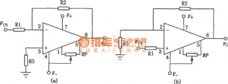
μA741 is a high performance, internal compensation operational amplifier. The features are: Low power consumption, no external frequency compensation. It is with offset voltage short circuit protection and offset voltage zeroing capacity. It will not appear latch phenomenon when it is working. It can be used as integrator, summing amplifier and general feedback amplifier. The similar or direct substitution models are: CF741MT, CF741CT, CF741MD, CF741CD, CF741MJ, CF741CJ, CF741CP, F007, F008 and so on. The μA741 typical application circuit is shown as above. Figure (a) is the inverting input amplifier circuit, Figure (b) is the same phase input amplifier circuit. (View)
View full Circuit Diagram | Comments | Reading(1085)
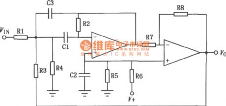
CF7631 series dual power high input impedance three op amp circuit diagram
Published:2011/5/13 4:21:00 Author:Rebekka | Keyword: dual power high input, impedance three op amp
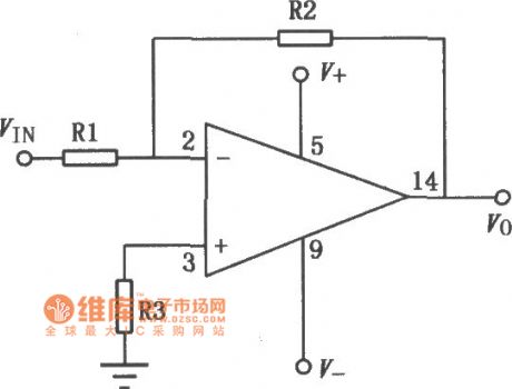
CF7631 is a CMOS low-power three-op amp. The features are: High input resistance, small input current, low power consumption, high gain. It is with frequency compensation, non-zero offset end, peripheral bias control. Its working voltage is ± 0. 5V ~ ± 8V. Its similar or direct substitution models are: CF7631BMD, CF7631BCD, CF7631CMD, CF76321CCD, CF7631ECD, CF7631BMJ, CF7631BCJ, CF7631CMJ, CF7631CCJ, CF7631ECJ, CF7631BCP, CF7631CCP, CF76321ECP and so on. The typical application circuit is shown as above. (View)
View full Circuit Diagram | Comments | Reading(612)
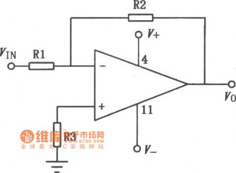
CM358 single power supply universal dual op amp circuit diagram
Published:2011/5/13 4:15:00 Author:Rebekka | Keyword: single power supply, universal dual op amp
CM358 is a high gain, contains two operational amplifier unit amplifiers. It is with no external frequency compensation. It only uses a single power supply and it has a low input current. It is usually used for transducer amplifier, the DC gain units and common signal processing circuit. Its similar or direct substitution models are: CFl58MT, CF258LT, CFl58MD, CF358CT, CF258LD, CF358CD, CFl58MJ, CF258LJ, CF358CJ, CF358CP, LM158 and so on. The typical application circuit is shown as above. (View)
View full Circuit Diagram | Comments | Reading(1100)
CF148 series dual power universal quad op amp circuit diagram
Published:2011/5/13 4:37:00 Author:Rebekka | Keyword: dual power universal, Quad op amp
CF148 series include four high-performance amplifier units. Each unit's performance is similar with gA741 op amp. It is with high gain, internal compensation, low power consumption, 4 op amp quiescent current phases are similar with μA741. This series uses internal accurate isolation technology. It is suitable for the occasions that requires multiple μA741. The similar or direct substitution models are: CFl48MD, CF248LD, CF348CD, CFl48MJ, CF248LJ, CF348CJ, CF348CP and so on. The typical application circuit is shown as above.
(View)
View full Circuit Diagram | Comments | Reading(613)
Panasonic NN-6270 microwave circuit diagram
Published:2011/5/16 3:48:00 Author:Ecco | Keyword: Panasonic , microwave
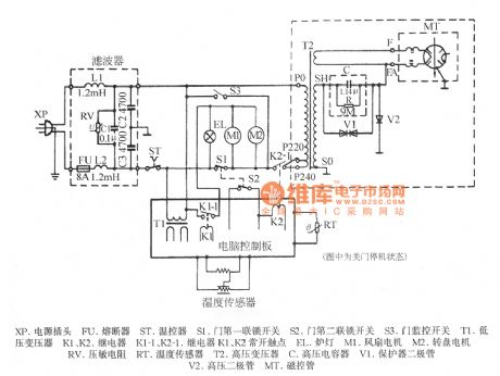
XP-power plug, FU-fuse, ST-temperature control, S1-door first interlock switch, S2-door second interlock switch, S3-threshold switch, T1-low-voltage transformer, K1, K2-relays, K1-1, K2-2- the normally open contacts of relay K1, K2, EL-furnace light, M1-fan motor, M2-wheel motor, RV-varistor, RT-temperature sensor, T2-high transformer, C-high-voltage capacitor, V1-protection diode, V2-high voltage diode, MT-magnetron
(View)
View full Circuit Diagram | Comments | Reading(4602)
UPS circuit with LM3524D
Published:2011/5/14 23:24:00 Author: | Keyword: LM3524D, UPS circuit
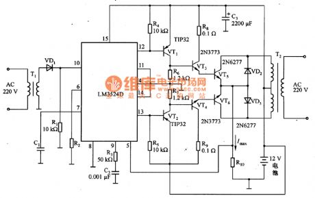
LM3524D is a kind of switch power supply controller which uses PWM operate mode. In the working mode, the pin 12 and pin 13 of LM3524D output pulse signals with the phase difference of 180°, whose voltages are amplified through VT1 and VT2 and then the electric currents are stimulated to be amplified by VT3 and VT4. As a result, both of the two processes drive the VT5 and VT6 to amplify the power of the pulse signals. The power amplifier VT5 and VT6 generates 12V square AV voltages on the one side of T2 transformer according to the alternating of the pulse signals outputting by VT1 and VT2.between turning on and turning off. After being stepped up, the square AV voltages are changed to 220 V AV voltages and are output through the other side of the transformer T2, which offer power supply for the load. The operating frequency of this circuit is decided by R2 and C1.VD2 and VD3 in this circuit is used to prevent the power amplifier from flowing through the current with a opposite direction. (View)
View full Circuit Diagram | Comments | Reading(3446)
Ward Caller Three
Published:2011/5/14 7:07:00 Author:Felicity | Keyword: Ward Caller,
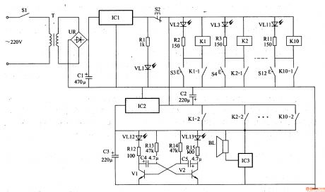
When the control buttons S3-S12 are not pressed, K1-K10 are both in the release state, Vl2-VL13 are off, BL is noiseless.
When one of the control buttons is pressed, the relay in this branch closes and is self-locked, and the LED shows the bed number. At the same time, the other group normally open contact closes to make the acoustic and optical alarm circuit work. VL12 and VL13 shines and BL sends a music alarm to remind the medical personnel to deal with it in time.
In practice, the number of relays, buttons, LEDs or current-limiting resistors can be adjusted according to the actual demand.
(View)
View full Circuit Diagram | Comments | Reading(547)
Ward Caller Two
Published:2011/5/14 6:41:00 Author:Felicity | Keyword: Ward Caller ,
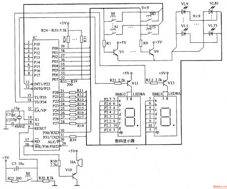
When one button of S1-S81 is pressed, the inside program control circuit of the IC detects the bed number represented by the button number. And the pin 16 is at low level to make V10 close, and HA sends out a call. Pin 15 and pin 14 are at low level to make V11 or V12 close. Pin 21-28 output signals to drive the digital code scope to display the calling bed number while the LED corresponding to the pressed button is on.
Once the reset button S0 is pressed, the lighted LED will be off, and the number displayed on the digital code scope will disappear, and HA will stop. (View)
View full Circuit Diagram | Comments | Reading(573)
Eyesight Protection Reminder
Published:2011/5/14 3:26:00 Author:Sue | Keyword: Eyesight, Protection, Reminder
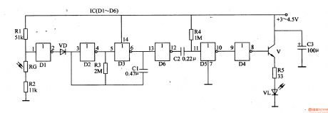
When the indoor light is strong, the inside resistance value of light sensitive resistor is small. IC's 1 pin has a low level, and 2 pin has a high level. VD is connected and the controlled pulse oscillator doesn't work, so VL is not illuminated. When the indoor light is so weak as to reach a certain level, NOT gate circuit D1 will reverse and make VD disconnected. The controlled pulse amplifier begins to work and generates square form pulse signal. The signal will turn into narrow pulse signal after differentiating circuit and shaping circuit. Then after the signal is amplified by V, it will promote VL to work and twinkle with a certain frequency. (View)
View full Circuit Diagram | Comments | Reading(496)
Multifunctional Alarm
Published:2011/5/14 3:06:00 Author:Sue | Keyword: Multifunctional, Alarm
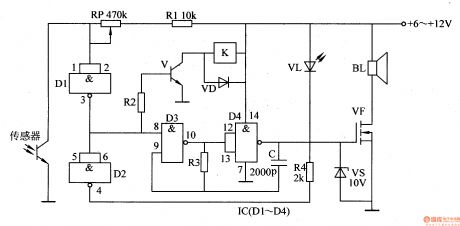
When the sensor detects nothing from outside, D1's input terminal is high level, while its output terminal is low level. D2 outputs high level, and VL is not illuminated. V is disconnected, and K is released. Audio oscillator composed of D3,D4,R3,C doesn't work and BL makes no sound.
When the sensor is stimulated, D1's input terminal turns into low level, and its output terminal becomes high level, which makes V begin to oscillate. The audio signal will force BL to make a warning sound after the signal is amplified by VF. (View)
View full Circuit Diagram | Comments | Reading(509)
main control panel of air conditioner circuit
Published:2011/5/15 6:22:00 Author:chopper | Keyword: main control panel, air conditioner
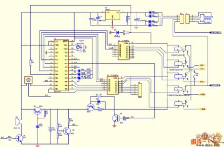
View full Circuit Diagram | Comments | Reading(811)
crystal diode DDZX96691TS internal circuit
Published:2011/5/16 3:14:00 Author:chopper | Keyword: crystal diode, internal
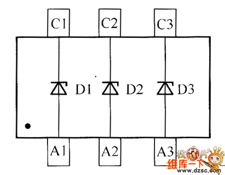
crystal diode DDZX96691TS internal is shown as following picture:
(View)
View full Circuit Diagram | Comments | Reading(488)
| Pages:1873/2234 At 2018611862186318641865186618671868186918701871187218731874187518761877187818791880Under 20 |
Circuit Categories
power supply circuit
Amplifier Circuit
Basic Circuit
LED and Light Circuit
Sensor Circuit
Signal Processing
Electrical Equipment Circuit
Control Circuit
Remote Control Circuit
A/D-D/A Converter Circuit
Audio Circuit
Measuring and Test Circuit
Communication Circuit
Computer-Related Circuit
555 Circuit
Automotive Circuit
Repairing Circuit