
Signal Processing
Index 94
105_MHz_to_107_MHzmixer_using_a_3N211_dual_gate_MOSFET
Published:2009/7/20 22:52:00 Author:Jessie
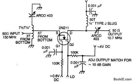
105 MHz to 10.7 MHzmixer using a 3N211 dual-gate MOSFET(courtesy Texas Instruments Incorporated). (View)
View full Circuit Diagram | Comments | Reading(673)
Electronic_organ_master_oscillator_using_an_ECG1026_thin_film_hybrid_module
Published:2009/7/20 22:51:00 Author:Jessie
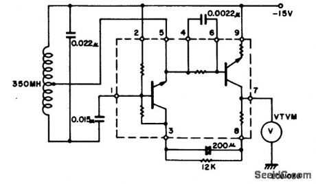
Electronic organ master oscillator using an ECG1026 thin-film hybrid module. Output is taken at pin 7, where the VTVM is shown connected to test output voltage level (courtesy GTE Sylvania Incorporated). (View)
View full Circuit Diagram | Comments | Reading(684)
10_MHz_oscillator_using_a_single_ECG703A_chip_that_can_be_used_as_a_short_range_transmitter
Published:2009/7/20 22:50:00 Author:Jessie
10 MHz oscillator using a single ECG703A chip that can be used as a short range transmitter. it is possible to modulate the oscillator by inserting the audio modulator shown between pin 1 and the tank circuit (courtesy GTE Sylvania Incorporated). (View)
View full Circuit Diagram | Comments | Reading(609)
Frequency_synthesizer_using_internal_time_base
Published:2009/7/20 22:45:00 Author:Jessie
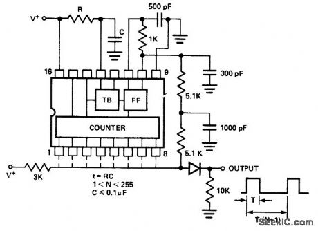
Frequency synthesizer using internal time base. The counter shown is an Intersil 8240 programmable timer/counter. The output of the circuit is a positive pulse train with a pulse width equal to T and a period equal to (N+1) T, where N is the programmable count between 1 and 255. The modulus N is the total count corresponding to the counter outputs connected to the output bus. For example if pins 1, 3 and 6 are connected to the output bus the total count is N =1+4+32=37 and the period of the output waveform is equal to (N+1) T or 38T. And T=RC (courtesy Intersil, Inc.). (View)
View full Circuit Diagram | Comments | Reading(794)
256_LEVEL_HOLD
Published:2009/7/20 21:32:00 Author:Jessie
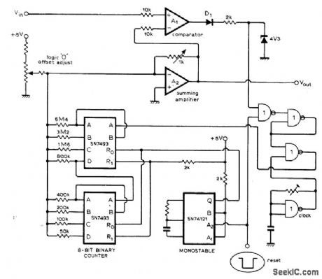
Uses digital approximation to hold sampled analog voltage for long periods. Cascaded SN7493 ICs form 8-bit binary counter providing 256 discrete voltage levels from opamp A2, while input voltage provides varying reference to opamp A1 serving as comparator. Apply0 at reset input to clear counter for period determined by monostable IC. Counter now feeds staircase waveform to A1 through A2 until staircase reaches Vin, when counter goes high and disables counter clock. Count is then held and sampled voltage appears at output.-N. Macdonald, Digital Sample and Hold, Wireless World, May 1976, p 78. (View)
View full Circuit Diagram | Comments | Reading(1334)
AUTOMATIC_FRINGE_TUNING
Published:2009/7/20 21:06:00 Author:Jessie
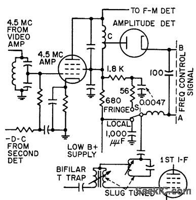
Circuit serves to disable sound track, to increase amplitude of sound carrier, so weak picture car tier will be tuned higher on i-f pass band, at point of desired fringe tuning.-C. W. Baugh, Jr. and L. J. Sienkiewicz, Sound Signal Tunes Tv Automatically, Electronics, 31:17, p 54-58. (View)
View full Circuit Diagram | Comments | Reading(664)
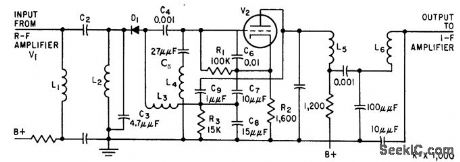
DIODE_MIXER_FOR_TUNER
Published:2009/7/20 21:05:00 Author:Jessie

1N87 semiconductor diode mixer D1 improves isolation of r-f amplifier from 6ER5 tube V2, connected as Colpitts oscillator.-E. H. Hugenholtz, 0ne-Tube Oscillator Mixers for Tv and F-M Tuners, Electronics, 33:3, p 76-79. (View)
View full Circuit Diagram | Comments | Reading(760)
STABILIZED_HORIZONTAL_OSCILLATOR
Published:2009/7/20 21:04:00 Author:Jessie
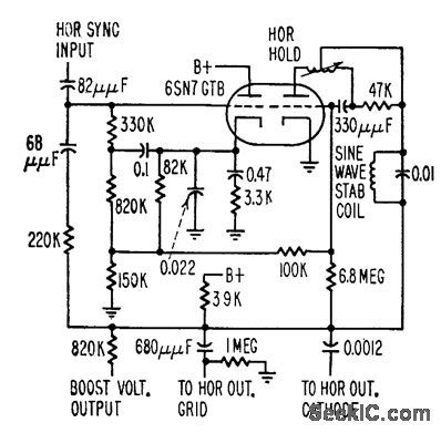
Sine-wave stabilization or ringing coil pulls Synchroguide horizontal oscillator frequency back to correct value when lube or other components drift in value.-W. E. Babcock, Unusual Tube Effects Cause Circuit Troubles, Electronics, 31:37, p 90-93. (View)
View full Circuit Diagram | Comments | Reading(1076)
SSB_GENERATORS
Published:2009/7/8 23:37:00 Author:May
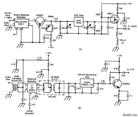
These two circuits are SSB generators. One uses a crystal filter by KVG Electronics at 9 MHz, theother uses a 455-kHz mechanical filter. By feeding the outputs into a mixer, the frequency of the SSBgenerator can be converted to other frequencies.Keep signal levels low enough so that distortion does notoccur. (View)
View full Circuit Diagram | Comments | Reading(1090)
PROGRAMMABLE_FREQUENCY_SINE_WAVE_OSCILLATOR
Published:2009/7/9 1:26:00 Author:May
This Wien-bridge oscillator is very popular for signal generators, since it is easily turned over a wide frequency range, and has a very low distortion sine-wave output. The frequency determining networks can be designed from about 10 Hz to greater than 1 MHz; the output level is about 6.0-V rms. By substituting a programmable attenuator for the buffer amplifier, a very versatile sine-wave source for automatic testing, etc. can be constructed.
(View)
View full Circuit Diagram | Comments | Reading(940)
HC_BASED_OSCILLATORS
Published:2009/7/9 1:24:00 Author:May
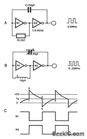
Two inverters, one resistor, and one capacitor are all that is required to make a HC(T)-based oscillator that gives reliable operation up to about 10 MHz. The use of two HC inverters produces a fairly symmetrical rectangular output signal. In the same circuit, HCT inverters give a duty factor of about 25%, rather than about 50%, since the toggle point of an HC and an HCT inverter is 1/2 VCC, and slightly less than 2 V, respectively. If the oscillator is to operate above 10 MHz, the resistor is replaced with a small inductor, as shown in Fig.68-4B.
The output frequency of the circuit in Fig. 68-4A is given as about 1/1.8rc, and can be made variable by connecting a 100-KΩ potentiometer in series with R. The solution adopted for the oscillator in Fig. 68-4B is even simpler: C is a 50-pF trimmer capacitor.
(View)
View full Circuit Diagram | Comments | Reading(891)
RLC_OSCILLATOR
Published:2009/7/9 1:23:00 Author:May
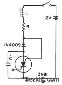
A positive transient, such as the power switch closing, charges C through L to a voltage above the supply voltage, if Q is sufficient. When the current reverses, the diode blocks and triggers the SCS. As the capacitor discharges, the anode gate approaches ground potential, depriving the anode of holding current. This turns off the SCS, and C charges to repeat the cycle. (View)
View full Circuit Diagram | Comments | Reading(847)
RECORDING_MANOMETER
Published:2009/7/20 20:49:00 Author:Jessie
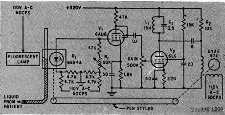
Pressure of blood or other body liquids is measured and recorded by photoelectric system.Mercury or other opaque fluids may also be measured. Servo loop maintains photocell at meniscus level of liquid,Mechanicallinkagealso drives recorder stylus,-W. E. Gilson and H.Ludwig, Recording Manometer Electronics,32:52,p 41. (View)
View full Circuit Diagram | Comments | Reading(717)
SLOW_SCAN_TV_RECEIVER
Published:2009/7/20 20:48:00 Author:Jessie
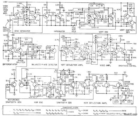
Signals from f-m telemetry system in balloon are picked up by commercial receiver and fed to distribution amplifier serving three monitors, having identical circuits as shown. Video band-width is 200 kc.-L. E. Flory et al., Television System for Stratoscope I, Electronics, 33:25, p 49-53.
(View)
View full Circuit Diagram | Comments | Reading(1672)
FIXED-FREQUENCY_VARIABLE_DUTY_CYCLE_OSCILLATOR
Published:2009/7/9 1:21:00 Author:May
In a basic astable timer,configuration periods t1 and t2 are not controlled independently. The lack of control make it difficult to maintain a constant period,T,if either t1 or t2 is varied.In this circuit,charge RAB and discharge RBC resistance are determined by the position of common wiper arm B of the Potentiometer so,it is possible to adjust the duty-cycle by adjusting t1 and t2 Proportionately,without changing period T.
At start-up,the voltage across G is less than the trigger level voltage (1/2 VDD),causing the timer to be triggered via pip 2,The output of the timer at m 3 Increases,turning off the discharge transistor at pin 7 and allowina Ct to charge through diode D1 and resitance RAB.When capacitor Ct charges to upper threshold voltage 2/3 VDD,the flip-flop is reset and the output at pin 3 decreases through diode D2 and resistor RBC.When the voltage at pin 2 reaches 1/3 VDD,the lower threshold or trigger level,the timer triggers.again and the cycle is repeated.In this circuit,the oscillator frequency remains fixed and the duty cycle is adjustable from less than 0.5% to greater than 99.5%. (View)
View full Circuit Diagram | Comments | Reading(1417)
Multicrystal_RF_oscillator_for_the_100_kHz_to_20_MHz_range
Published:2009/7/20 23:46:00 Author:Jessie
Multicrystal RF oscillator for the 100 kHz to 2.0 MHz range (courtesy Motorola Semiconductor Products Inc.). (View)
View full Circuit Diagram | Comments | Reading(738)
DIAMOND_MODULATOR
Published:2009/7/20 23:48:00 Author:Jessie
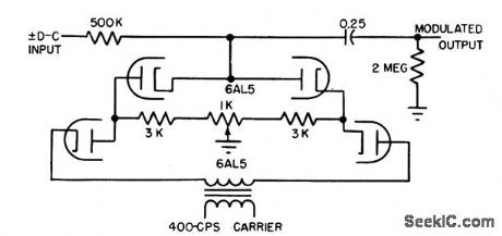
Carrier signal turns electron tube or equivalent crystal diode on and off to modulate d-c input signal. Signal-noise ratio is about 1,500 to 1, with carrier voltage of 19V rms. Output is linear up to 3 V rms for d-c inputs up to 10 V.-L. S.Klivans, Modulators for Automatic Control Systems, Electronics, 31:1, p 82-84. (View)
View full Circuit Diagram | Comments | Reading(724)
DIRECT_R_C_COUPLED_COMMON_EMITTER_MODULATOR
Published:2009/7/20 23:50:00 Author:Jessie
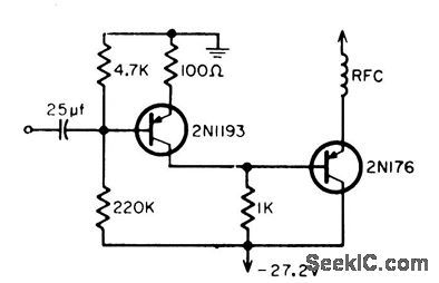
Performance is considerably better than that of conventional trans. former-coupled collector-modulated 27-Mc CB modulator. Total current drain is 83 ma.0.14 v gives full modulation. Power gain is nearly 20 db for 2N1193. Requires no audio transformers.-B. Rheinfelder, Modulation Techniques for Transistorized A-M Transmitters, EEE, 11:7, p 54-57. (View)
View full Circuit Diagram | Comments | Reading(670)
PLL_frequency_synthesizer_with_109_MHz_to_12399_MHz_output
Published:2009/7/20 23:52:00 Author:Jessie
PLL frequency synthesizer with 10.9 MHz to 12.399 MHz output. This circuit is designed to generate at 10.7 MHz IF over the 200 kHz to 1699 kHz band for an ADF. Steps are 1 kHz apart (courtesy Motorola Semiconductor Products Inc.). (View)
View full Circuit Diagram | Comments | Reading(3686)
MODEM_PULSE_SHAPER
Published:2009/7/20 23:52:00 Author:Jessie
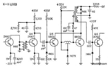
Removes audio component from modulator output to prevent crosstalk, and shapes pulse to required rise and fall lime and width. Used in four-channel ppm microwave multiplex unit.-P. W. Kiesling, Jr., Portable Multiplexor for Telephone Communications, Electronics, 32:2; p 60-62. (View)
View full Circuit Diagram | Comments | Reading(637)
| Pages:94/195 At 2081828384858687888990919293949596979899100Under 20 |
Circuit Categories
power supply circuit
Amplifier Circuit
Basic Circuit
LED and Light Circuit
Sensor Circuit
Signal Processing
Electrical Equipment Circuit
Control Circuit
Remote Control Circuit
A/D-D/A Converter Circuit
Audio Circuit
Measuring and Test Circuit
Communication Circuit
Computer-Related Circuit
555 Circuit
Automotive Circuit
Repairing Circuit