
Signal Processing
Index 80
BRIDGED_T_AUDIO_OSCILLATOR
Published:2009/7/19 21:43:00 Author:Jessie
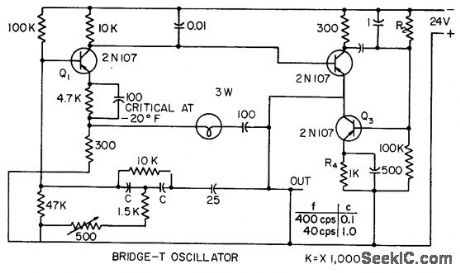
Incorporates heavy degenerative feedback in which small lamp is nonlinear compensating resistance. Provides constant output frequency and voltage for any supply between 12 and 32 V, at temperatures down to -20°F. Frequency is determined by capacitors C and 500-ohm trimmer control, to give choice of 100, 150, 230, and 350 cps.-H. P. Van Eckhardt, Crevasse Detector Blazes Glacial Trails, Electronics, 31:3, p 63-65. (View)
View full Circuit Diagram | Comments | Reading(743)
122_KC_GROUNDED_COLLECTOR_HARTLEY
Published:2009/7/19 22:08:00 Author:Jessie
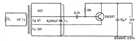
Simple class-C L-C arrangement has many advantages for power oscillators and for d-c to a-c converters. One side of tank can be grounded.-P. Laakmann, Designing Class. C Transistor L-C Oscillators, Electronics, 35:30, p 42-45. (View)
View full Circuit Diagram | Comments | Reading(744)
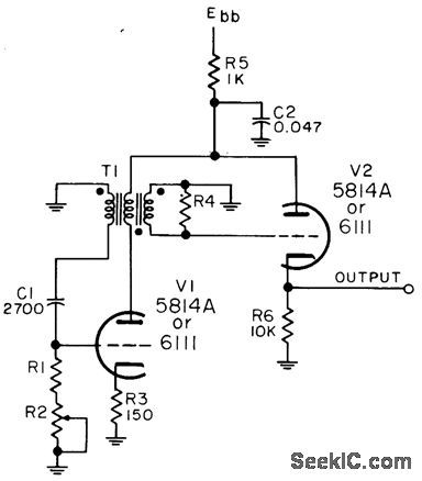
PERFERRED_PULSE_FREQUENCY_DIVIDER_
Published:2009/7/19 21:50:00 Author:Jessie
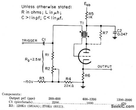
Blocking oscillator design produces equally spaced pulses at submultiple of 2 to 5 of trigger frequency. Maximum prf is 2,000 pps. Input und output are both positive. Plate voltage is 300 V with 5814A tube and 150 V with 6111. R6 is 100 or 150 ohms depemding on tube. R7 should be maximum that will just suppress ringing,-NBS, Handbook Preferred Circuits Navy Aeronautical Electronic Equipment, Vol. I, Electron Tube Circuits, 1963, PC 50, p 50-2. (View)
View full Circuit Diagram | Comments | Reading(758)
SIMPLE_TTL_LSTTL_CMOS_SQUARE_WAVE_GENERATORS
Published:2009/7/10 3:43:00 Author:May
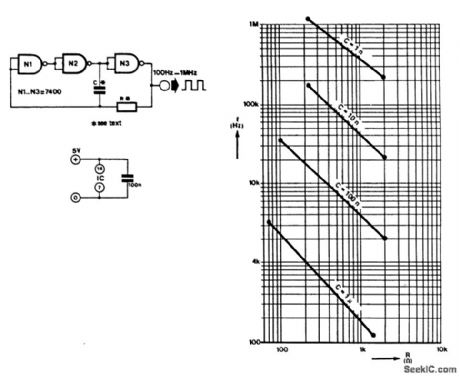
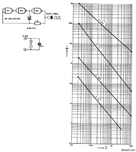

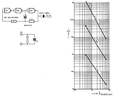
These three circuits for TTL. LSTTL. and CMOS logic use three gates each, and one or two resistors and capacitor as a square-wave oscillator. The circuits are useful for clock oscillators, etc. R and C are determined from the nomographs (View)
View full Circuit Diagram | Comments | Reading(1625)
WIEN_BRIDGE_OSCILLATOR
Published:2009/7/10 3:26:00 Author:May
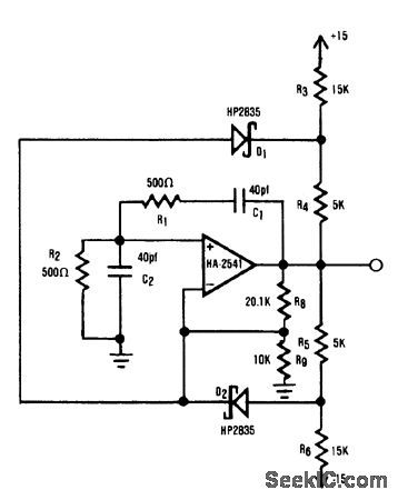
The HA2541 is well-suited for use as the heart of an oscillator. In spite of the rudimentary diode limit-ing that is provided by R3 through R7 and Dl and D2, a good-quality sine wave of 40 MHz is readily attain-able with an upper limit of 50 MHz, which exceeds the unity-gain bandwidth of HA-2541.
R1/C1 and R2/C2 provide the required regenerative feedback needed for adequate frequency stability.In theory, the feedback network requires a gain of three to sustain oscillation. However,the practical gain needed is just over three and is provided by R8 and R9. (View)
View full Circuit Diagram | Comments | Reading(0)
RELAXATION_OSCILLATOR
Published:2009/7/10 3:23:00 Author:May
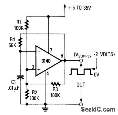
This oscillator runs at about 150 Hz, but C1 and/or R4 can be proportionately changed to alter this frequency. Rise and fall times are 12 and 7 μs, respectively. (View)
View full Circuit Diagram | Comments | Reading(1055)
CODE_PRACTICE_OSCILLATORⅠ
Published:2009/7/10 3:20:00 Author:May
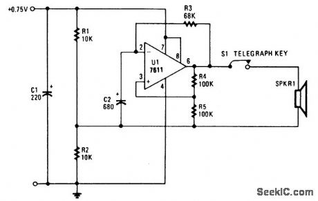
U1 is used as an oscillator; the frequency is determined by C2 and R3.Use an 80 Ω or similar highimpedance speaker, and a 1.5-V battery for a power source. (View)
View full Circuit Diagram | Comments | Reading(697)
STAIRCASE_GENERATOR
Published:2009/7/10 3:15:00 Author:May
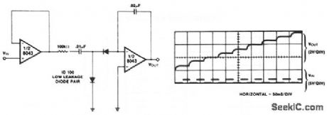
This circuit is a high-input impedance version of the so-called diode pump or staircase generator. Note that charge transfer takes place at the negative-going edge of the input signal. The most common application for staircase generators is in low-cost counters. By resetting the capacitor when the output reaches a predetermined level, the circuit can be made to count reliably up to a maximum of about 10. (View)
View full Circuit Diagram | Comments | Reading(0)
AUDIO_OSCILLATOR
Published:2009/7/10 3:14:00 Author:May
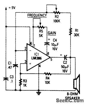
The circuit's frequency oscillation is f=2.8/ [C1x(R1+R2)]. Using the values shown, the out-put frequency can be varied from 60 Hz to 20 kHz by rotating potentiometer R2.
A portion of IC1's output voltage is fed to its noninverting input at pin 3. The voltage serves as a reference for capacitor C1, which is connected to the noninverting input at pin 2 of the IC. That capacitor continually charges and discharges around the reference voltage, and the result is a square-wave output. Capacitor C2 decouples the output. (View)
View full Circuit Diagram | Comments | Reading(0)
AUDIO_MODULATED_1_MC_TUNED_TD_OSCILLATOR
Published:2009/7/19 22:27:00 Author:Jessie
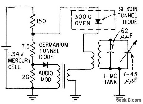
Uses silicon tunnel diode that, with no surface protection, may be dipped in liquid nitrogen, placed in furnace, or immersed in acid, with only minor change in oscillator and modulation frequencies.-I. A. Lesk, N. Holonyak, Jr., and U. S. Davidsohn, The Tunnel Diode-Circuits and Applications, Electronics, 32:48, p 60-64. (View)
View full Circuit Diagram | Comments | Reading(805)
μA2240_STAIRCASE_GENERATOR
Published:2009/7/10 3:08:00 Author:May

The μA2240 timer/counter, combined with a precision resistor ladder network and an op amp, form the staircase generator. In the astable mode, once a trigger pulse is applied, the μA2240 operates continuously until it receives a reset pulse. The trigger input at pin 11 is tied to the time base output at pin 14, resulting in automatic starting and continuous operation. The frequency of the time-base oscillator, TBO, is set by the time constants R1 and C1 ( f=1/R1C1). For this example, a 10-KΩ) resistor and a 0.01-μF capacitor form the timing network.The counter outputs are connected to a precision resistor ladder network with binary-weighted resistors. The current sink through the resistors connected to the counter outputs correspond to the count number. For example, the current sink at Q7, the most significant bit, is 128 times the current sink at Q0, the least significant bit. As the count is generated by the μA2240 eight-bit counter, the current sink through each active binary-weighted resistor decreases the positive output of the op amp in discrete steps.The feedback potentiometer is set at a nominal 10 KΩ to supply a maximum output voltage range. An input of 12 V allows a 10-V output swing. With a 0.5-V input reference on pin 3 of the TCL271, the output will change front 10.46 V maximum, in 256 steps of 38.9 mV per step, to a 0.5 V minimum. Each step has a pulse duration of 100 μs and an amplitude decrease of 38.9 mV. The waveform output is repeated until a reset is applied to the μA2240. (View)
View full Circuit Diagram | Comments | Reading(1360)
PREFERRED_ASTABLE_BLOCKING_OSCILLATOR
Published:2009/7/19 22:25:00 Author:Jessie
Used as pulse generator when frequency stability is not important. Output can be used as trigger without further shaping. R4 should be maximum that will just suppress ringing. Design equations are given for R1 and R2, but final values must be determined experimentally. Range is 200 to 2,000 pps. Output is positive.-NBS, Handbook Preferred Circuits Navy Aeronautical Electronic Equipment, Vol, I, Electron Tube Circuits, 1963, PC 48, p 48-2. (View)
View full Circuit Diagram | Comments | Reading(1017)
CODE_PRACTICE_OSCILLATOR_Ⅲ
Published:2009/7/10 3:07:00 Author:May
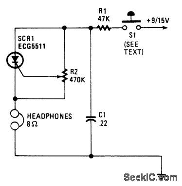
Capacitor C1 charges through resistor R1, and when the gate level established by potentiometer R2 is high enough, the SCR is triggered. Current flows through the SCR and earphones, discharging C1. The anode voltage and current drop to a low level, so the SCR stops conducting and the cycle is repeated. Resistor R2 lets the gate potential across C1 be adjusted, which charges the frequency or tone, Use a pair of 8-Ω headphones. The telegraph key goes right into the B+ line, 9-V battery. (View)
View full Circuit Diagram | Comments | Reading(640)
8_to_170_KC_WITH_PLUG_IN_CRYSTALS
Published:2009/7/19 22:23:00 Author:Jessie
Oscillator frequency can be changed by replacing crystal and one capacitor in feedback loop. Stability is obtained from squaring transistor Q1 which feeds crystal.-R. Couvela, Oscillator Frequency is Changed by Plug-In Units, Electronics, 34:36, p 86-87. (View)
View full Circuit Diagram | Comments | Reading(724)
AUDIO_OSCLLATOR
Published:2009/7/10 3:03:00 Author:May
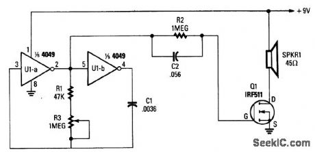
Two gates, U1A and U1B (1/3 of a 4049 hex inveter), are connected in a VFO circuit. Components R1, R3, and C1 set the frequency range of the VFO. With the values given, the circuit's output can range from a few hundred hertz to over several thousand hertz by adjusting R3.
The simplest way to change the frequency range of the oscillator is to use different capacitance values for C1. A rotary switch, teamed up with a number of capacitors, can be used to select the desired fre-quency range. (View)
View full Circuit Diagram | Comments | Reading(939)
CRYSTAL_OSCILLATOR
Published:2009/7/10 3:02:00 Author:May
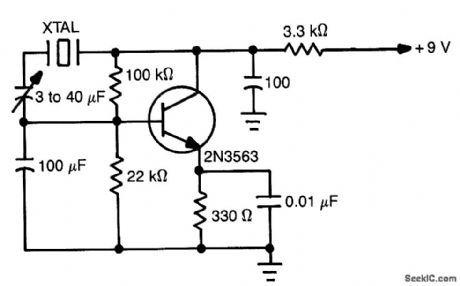
This simple circuit will oscillate with a wide range of crystals. Connect several different types of cystal holders in parallel to improve versatility. The 3-to 40-pF capacito adjusts crystal frequency over a small range for setting standard-frequency transmissions when the unit is used as a crystal calibrator. (View)
View full Circuit Diagram | Comments | Reading(0)
CRYSTAL-CONTROLLED_BRIDGE_OSCILLATOR
Published:2009/7/10 3:00:00 Author:May
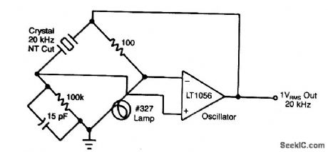
This crystal-controlled oscillator uses the current variations in a small lamp to stabilize amplitude variations. (View)
View full Circuit Diagram | Comments | Reading(697)
PHASE_LOCKED_20_MHz_OSCILLATOR
Published:2009/7/10 2:59:00 Author:May
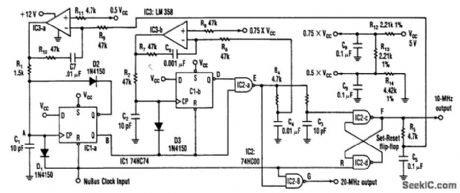
This circuit produces a 20-MHz clock phase locked to a 10-MHz dock present in the Apple MAC II.To generate the 20-MHz signal, the circuit produces a 25 ns negative-going pulse delayed 50 ns from the falling edge of the 10-MHz Nubus clock input at point E. NORing that pulse with the Nubus clock produces the 20-MHz clock at point G. Applying the 25-ms pulse to the set input of an S/R flip-flop and the Nubus clock to the reset input results in a 10-MHz square wave at F. (View)
View full Circuit Diagram | Comments | Reading(1455)
1_to_20_MHz_TTL_OSCILLATOR
Published:2009/7/10 2:59:00 Author:May
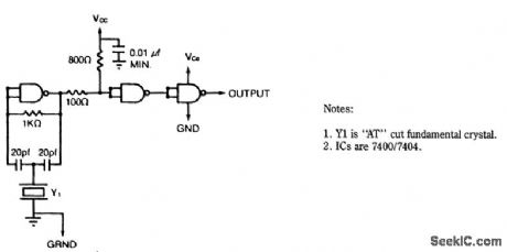
View full Circuit Diagram | Comments | Reading(776)
CRYSTAL_MOS_FET
Published:2009/7/19 22:19:00 Author:Jessie
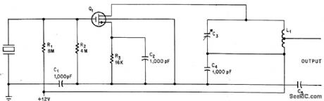
Oscillation is maintained even with 100-microvolt oscillator output signal when using mos fet.-G. G. Luettgenau and S. H. Barnes, Designing With Low-Noise MOS FETs: A Little Different But No Harder, Electronics, 37:31, p 53-58. (View)
View full Circuit Diagram | Comments | Reading(875)
| Pages:80/195 At 206162636465666768697071727374757677787980Under 20 |
Circuit Categories
power supply circuit
Amplifier Circuit
Basic Circuit
LED and Light Circuit
Sensor Circuit
Signal Processing
Electrical Equipment Circuit
Control Circuit
Remote Control Circuit
A/D-D/A Converter Circuit
Audio Circuit
Measuring and Test Circuit
Communication Circuit
Computer-Related Circuit
555 Circuit
Automotive Circuit
Repairing Circuit