
Signal Processing
Index 72
TRANSISTORIZED_FREE_RUNNING_CASCODE_MULTIVIBRATOR
Published:2009/7/16 11:27:00 Author:Jessie
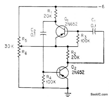
Output waveform can be rectangular or sawtooth, with polarity depending on setting of potentiometer. -C. Sing, Advantages of Free-Running Cascade Multivibrators, Electronics, 37:5, p 28-29. (View)
View full Circuit Diagram | Comments | Reading(980)
VARIABLE_POWER_ONE_SHOT
Published:2009/7/16 10:55:00 Author:Jessie
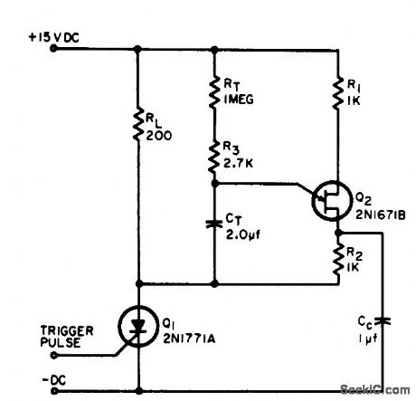
Switches load currents from few ma to over 1 amp for precise time interval ranging from few millisec to one minute. Is excellent solid-state substitute for slug relays, dashpots, and thermal timers. Several stages can be cascaded to form sequence timer. With values shown, and RT at 680K, 1-V trigger pulse initiates 1-sec on period.-J. C. Rich and R. D. Turner, Variable Time, Power One-Shot Multivibrator, EEE, 12:7, p 25-26. (View)
View full Circuit Diagram | Comments | Reading(882)
REDUCING_RESET_POWER_LEVEL
Published:2009/7/16 10:53:00 Author:Jessie
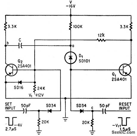
Addition of diode D1 to conventional mvbr decreases required amplitude and duration of reset pulse. -H. Inose and T. Tomiyama, Diode Lowers Multi's Reset Power Level, Electronics, 39:13, p 76-77. (View)
View full Circuit Diagram | Comments | Reading(832)
CONTINUOUSLY_VARIABLE_PRR
Published:2009/7/16 10:46:00 Author:Jessie
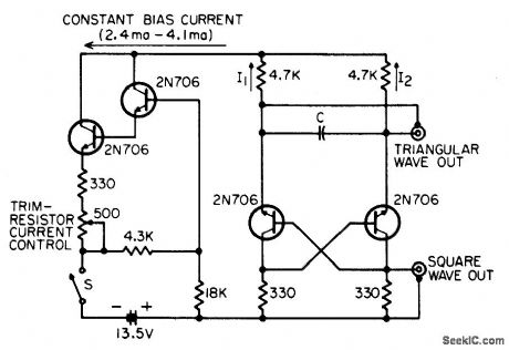
When basic mvbr is biased from constant-current source, tops of square wave become flat across collector resistor, and triangular wave across capacitor becomes linear. Pulse repetition rate then varies directly with magnitude of constant biasing current, over range of 5.6 cps to 2.68 Mc, by using only seven different capacitance values for C (from 330 pf to 100 mfd).-J. H. Bayne, Jr., and R. J. Haislmaier, Improved Multi with Continuously Variable Rep Rate, EEE, 13:5, p 44-45. (View)
View full Circuit Diagram | Comments | Reading(981)
TIME_AND_PERIOD_ADAPTER
Published:2009/7/16 20:10:00 Author:Jessie
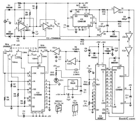
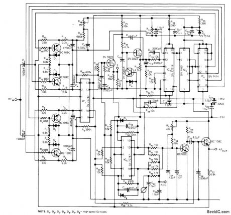
This circuit enables time period measurements to be made on a DMM. Integrated circuit IC1, an LM311 comparator, conditions the input waveform for the 5-V logic required by the circuit. The gate signal is applied to IC7, a CD4040B CMOS 12-stage binary counter, to measure pulse width, or through IC5, a CD4013B CMOS dual flip-flop, to measure time period. Integrated circuit IC2, a CD4069UB CMOS hex inverter, provides the precision 2.000-MHz crystal-controlled pulse train for IC3, a CMOS divide-by-N counter. It divides the pulse train by 1, 10,100,1000,or10,000 to cover the five ranges selected by rotary selector switch 52. The divider's output is gated by the input pulse at IC7 through a resistor-diode NOR gate. Integrated circuit IC4, a 78L05 voltage regulator, supplies +5V to the circuit; IC2-d, IC2-e, and IC2-f provide the properly timed RESET signal for IC7 and the LATCH ENABLE signal for IC6, an AD567 digital-to-analog converter (DAC), the key component in this adapter. DAC IC6 converts the 12-bit count stored in IC7 to a negative output current. That current is converted to a negative voltage by the combination of R13 and R14. The voltage is sent to a DMM at jack J2 over a twisted-wire pair terminated with a phono plug at one end and a suitable matching plug for the DMM at the other end. (View)
View full Circuit Diagram | Comments | Reading(1684)
AM_DEMODULATOR
Published:2009/7/16 7:00:00 Author:Jessie
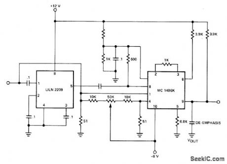
Signetics ULN2209 IC provides 55-dB gain for input signal and sym-metrical limiting above 400 μV. Limited carrier is then applied to MC1496K balanced modulator-demodulator transistor array for demodulation. Output filtering is required to remove high-frequency sum components of carrier from audio signal. Output amplitude is maximum when phase difference between signal and carrier inputs is 0°.- Signetics Analog Data Manual, Signetics, Sunnyvale, CA, 1977, p 757-758. (View)
View full Circuit Diagram | Comments | Reading(0)
LIMITER_DETECTOR
Published:2009/7/16 6:50:00 Author:Jessie

Used in all-band double-conversion superheterodyne receiver for AM, narrow-band FM, CW, and SSB operation. Q29 acts as limiter on FM but on AM is 455-kHz amplifier whose RF output is coupled to 1N60 AGC rectifier pair connected as voltage doubler that provides bias for AGC amplifier Q33-Q34. Output of Q29 is coupled to detector by T3. Although detector is actually phase discriminator, mode switch connects circuit as half-wave rectifier for AM and CW/SSB. On CW/SSB (S1 on 1), AGO rectifier is disconnected and AGC diodes receive bias from manual gain-control pot. BFO is then energized and connected to T3. Output of diode detector feeds squelch and audio stages. Supply is 13.6 V regulated. Article gives all circuits of receiver.-D. M. Eisenberg, Build This All-Band VHF Receiver, 73 Magazine, Jan.1975, p 105-112. (View)
View full Circuit Diagram | Comments | Reading(1662)
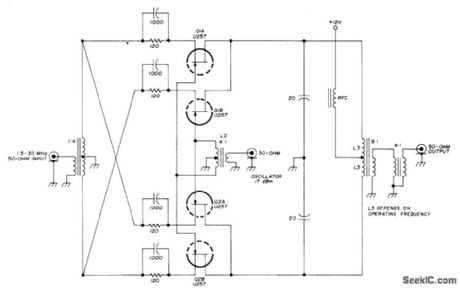
DOUBLE_BALANCED_MIXER_1
Published:2009/7/16 6:48:00 Author:Jessie
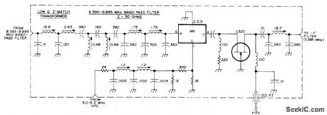

Uses Watkins-Johnson M6 low-level hot-carrier-diode double-balanced mixer as replacement for FET second mixer amateur-band dual-conversion receiver to reduce intermodulation distortion.U310, CP643, or CP651 can be used in place of U320 high-transconductance JFET. Pi-network output circuit couples 2000-ohm output of JFET stage to 2000-ohm IF filter. All inductance values are in microhenrys.-A. J. Burwasser, Reducing Intermodulation Distortion in High-Frequency Receivers, Ham Radio, March 1977, p 26-30. (View)
View full Circuit Diagram | Comments | Reading(2694)
100_MHz_MIXER
Published:2009/7/16 6:45:00 Author:Jessie
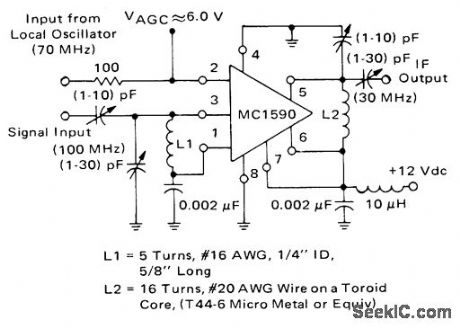
With local oscillator frequency of 70 MHz, opamp provides difference frequency of 30 MHz at high conversion gain. Isolation between oscillator and signal source is excellent.-B. Trout, A High Gain Integrated Circuit RF-IF Amplifier with Wide Range AGC, Motorola, Phoenix, AZ, 1975, AN-513, p 9. (View)
View full Circuit Diagram | Comments | Reading(1978)
2_METER_DUAL_VMOS
Published:2009/7/16 6:30:00 Author:Jessie
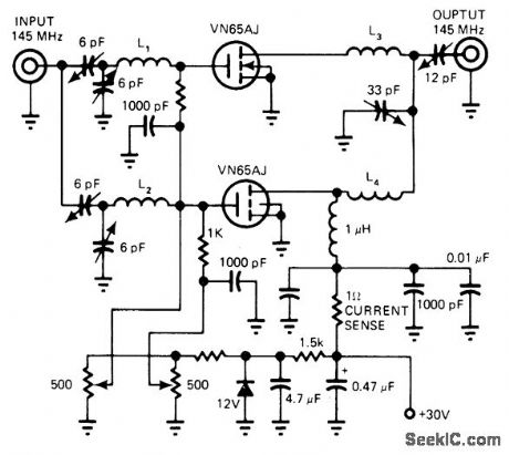
Provides 10-W PEP output at 146 MHz for amateur applications. Noise figure is only 2.35 dB, and two-tone IMD is -30 dBC.- E. Oxner, Will VMOS Power Transistors Replace Bipolars in HF Systems?, EDN Magazine, June 20, 1977, p 71-75. (View)
View full Circuit Diagram | Comments | Reading(853)
RF_PREAMP
Published:2009/7/16 6:17:00 Author:Jessie
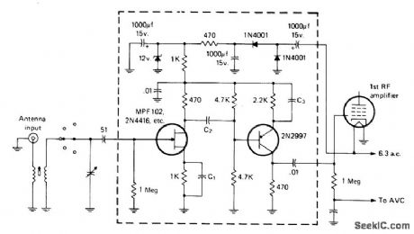
Boosts sensitivity of older tube-type communication receiver when added ahead of first RF tube. Has low noise figure. Values of C1, C2, and C3 are varied to suit receiver being used. Using 0.01 μF for these gives 20-dB gain from 0.5 to 30 MHz; if this overloads receiver on lower frequency ranges, try smaller values.-I. Math, Math's Notes, CQ, April 1975, p 37-38 and 62. (View)
View full Circuit Diagram | Comments | Reading(1584)
AF_FOR_AM_SSB_CW
Published:2009/7/16 6:07:00 Author:Jessie
Uses SG3402T as detector, with BFO disabled for AM. Pin 3 of detector output is main audio source, feeding preamp using half of dual opamp whose output goes to AF gain control except when CW filter is in use. Filter has two identical 400-1600 Hz active bandpass sections joined by threshold detector.LM38ON-8 AF power amplifier is rated at 600mW output. Audio from pin 8 of detector is amplified about 30 times in second half of dual opamp before rectification for use as AGC voltage. Circuit includes S-meter fed by AGO section. Article gives construction details of complete receiver.-R. Megifian, The Minicom Receiver, 73 Magazine, April 1977, p 136-149.
(View)
View full Circuit Diagram | Comments | Reading(1473)
BALANCED_FOUR_FET_MIXER
Published:2009/7/16 6:04:00 Author:Jessie
Uses two matched FET pairs to bring third-order inter-modulation distortion suppression down to 71 dB. Developed for use in high-quality communication receiver.-U. L. Rohde, Optimum Design for High-Frequency Communications Receivers, Ham Radio, Oct. 1976, p 10-25. (View)
View full Circuit Diagram | Comments | Reading(1138)
PLL_IN_AM_RECEIVER
Published:2009/7/16 5:58:00 Author:Jessie
Phase-locked loops provide required stability for synchronous detection to improve reception quality of commercial double-sideband AM transmissions. Signal input and output of VCO are multiplied in phase-sensitive detector or multiplier that produces voltage proportional to phase difference between input and VCO signals. After filtering and amplifying, this voltage is used to control frequency of VCO to make it synchronize with incoming signal. Features include absence of image responses since IF is 0 Hz, almost complete immunity to selective fading, and conversion of RF to audio at very low signal levels so overall receiver gain is achieved mainly in audio amplifier. Article traces development and operation of receiver in detail.-T. Mollinga, Solve Phase Stability Problem in AM Receivers with PLL Techniques, EDN Magazine, Feb. 20, 1975, p51-56. (View)
View full Circuit Diagram | Comments | Reading(1515)
CASCADED_ONE_SHOTS_GENERATE_PULSES_IN_BURST
Published:2009/7/16 5:50:00 Author:Jessie
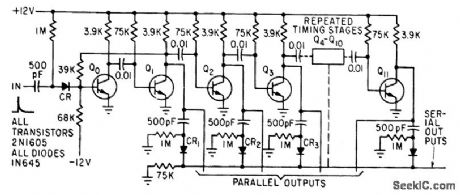
Addition of redundant stages to timing portion of conventional monostable mvbr permits generating bursts of eleven 2-kc pulses every 0.1 sec. Used for testing decimal counters at high counting rotes; each burst gives visible one-digit advance in readout because of 94.5-millisec time between bursts.-J. Gaon, Simple Counter Tester Uses Cascaded One-Shots, Electronics, 36:14, p 40-41. (View)
View full Circuit Diagram | Comments | Reading(688)
SYNC_BLOCKING_OSCILLATOR
Published:2009/7/16 21:20:00 Author:Jessie
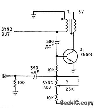
Free-running period of grounded-emitter stage is made to lock in with frequency of pulse generator, to provide synchronizing signal for conventional oscilloscope during tests of high-speed computer circuits.-L. Neumann, Transistorized Generator for Pulse Circuit Design, Electronics, 32:14, p 47-49. (View)
View full Circuit Diagram | Comments | Reading(989)
COLPITTS_ORYSTAL_OSCILLATOR
Published:2009/7/12 23:29:00 Author:May
This circuit is commonly called a Colpitts oscilLcttor. C1 and C2 determine the feedback ratio that maintains oscillation. To obtain maximum frequency stability and output level, C1 and C2 should be selected for a given frequency. (View)
View full Circuit Diagram | Comments | Reading(1066)
TTL_ORYSTAL_OSCILLATOR
Published:2009/7/12 23:28:00 Author:May
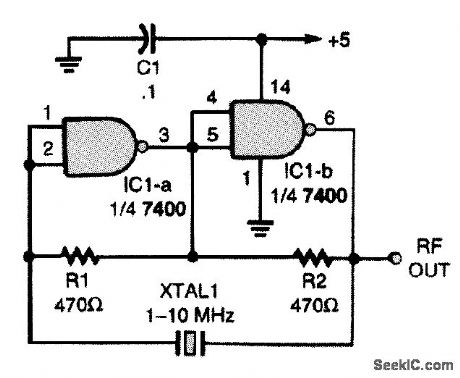
Here is an oscillator circuit that uses no L/C components. It uses two sections of a 7400 TTL IC, two resistors, and a crystal to make up a simple and stable oscillator circuit. (View)
View full Circuit Diagram | Comments | Reading(3036)
32768_kHz_MICROPOWER_OSCILLATOR
Published:2009/7/12 23:27:00 Author:May
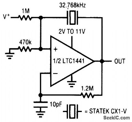
Using an LTC1441, this oscillator pulls 9 μA at a supply voltage of 2 V. The circuit has no spurious modes. (View)
View full Circuit Diagram | Comments | Reading(1484)
PULSE_HEIGHT_DISCRIMINATOR
Published:2009/7/16 21:14:00 Author:Jessie
Delivers trigger pulse when input signal reaches pre determined threshold. Used in nuclear counting experiments, in satellite and rocket applications where sensitivity and stability are essential.-R. Ii. Wagner, Stable, Sensitive Pulse Height Discriminator, EEE, 10:7, p 28-29. (View)
View full Circuit Diagram | Comments | Reading(1142)
| Pages:72/195 At 206162636465666768697071727374757677787980Under 20 |
Circuit Categories
power supply circuit
Amplifier Circuit
Basic Circuit
LED and Light Circuit
Sensor Circuit
Signal Processing
Electrical Equipment Circuit
Control Circuit
Remote Control Circuit
A/D-D/A Converter Circuit
Audio Circuit
Measuring and Test Circuit
Communication Circuit
Computer-Related Circuit
555 Circuit
Automotive Circuit
Repairing Circuit