
Signal Processing
Index 77
80_AND_160_m_DIRECT_CONVERSION_RECEIVER
Published:2009/7/17 3:24:00 Author:Jessie
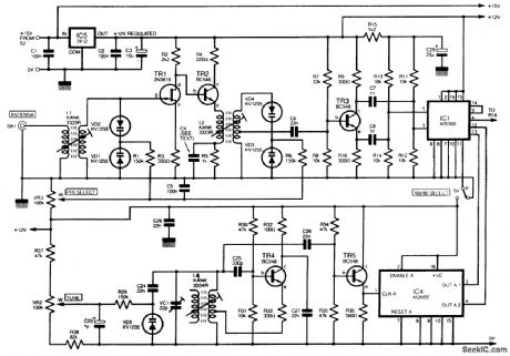
The full circuit diagram, except for power supply, for the direct-conversion top-band and 80-m receiver is shown. Incoming RF from the antenna is fed to the primary side of coil L1. This trans-former/coil is bought to resonance at the required frequency by a pair of back-to-back varicap diodes (VD1 and VD2). TRI, an RE, is coupled to the base (b) of transistor TR2, an emitter-follower. The output of TR2 feeds L2, the secondary being brought to resonance by varicaps VD3 and VD4. The variable-frequency oscillator (VFO) comprises a tuned circuit consisting of transformer L3, variable trimmer capacitor VC1, and varicap diode VD5. Variable bias to VD5 is provided by tuning control VR2. Transistor TR4 maintains oscillations at the desired frequency, and TR5 is an emitter-follower. The output of TR5 is sufficient to drive the CMOS divider chain formed by IC4. The VFO covers the frequency range 6.9 to 8.1 MHz, and this is divided by IC4 to produce 3450 to 4050 kHz for 80 m and 1725 to 2025 kHz for 160 m. The output of IC4 is fed to IC1, part of the product detector. The RF signal from the secondary tap on L2 is fed to a phase splitter formed around transistor TR3. Analog switch C1 operates at the selected VFO frequency and thus produces sum and difference frequencies of the VFO and the incoming RE. The output of IC1 at pin 4 is filtered to give resolved audio at this point. A high-gain inverting amplifier, with -3-dB points of approximately 300 Hz and 3 kHz, is formed by IC2a. This audio is now fed to IC3 with a maximum power output of 2 W. An LM380 is used in a standard configuration, and a fixed gain of around 30 dB is obtained. (View)
View full Circuit Diagram | Comments | Reading(2153)
SIGNAL_AVERAGER_CIRCUIT
Published:2009/7/17 3:24:00 Author:Jessie
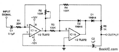
The first operational amplifier,IC1-a,is an inverthing amplifier whose gain can be adjusted up to 5.Adjustable feedback resistor R2 sets the circuit gain. The second amplifier,IC1-b,forms a half-wave rectifier and the signal averager clips the brief peaks and displays them over a longer period of time. (View)
View full Circuit Diagram | Comments | Reading(1024)
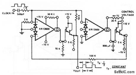
Triangular_square___wave_VCO
Published:2009/7/17 3:17:00 Author:Jessie
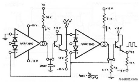
This classic triangular/square-wave generator (chapter 5) uses both sections of an XR-13600 (Fig. 11-1B). With the values shown, the oscillator provides signals from 200 kHz to below 2 Hz when IC is varied from 1 mA to 10 nA.The output amplitudes are set by IA×RA. Notice that the peak differential-input voltage must be less than 5 V to prevent zenering the inputs. EXAP Corporahon Databook 1990 p 5-255 (View)
View full Circuit Diagram | Comments | Reading(967)
VARIABLE_RESISTOR_CONTROLLED_REGENERATIVE_RECEIVER
Published:2009/7/17 3:16:00 Author:Jessie
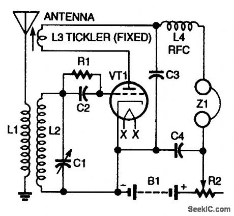
View full Circuit Diagram | Comments | Reading(760)
SCA_RECEIVER
Published:2009/7/17 3:15:00 Author:Jessie
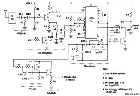
A simple PLL-based FM demodulator can be made to demodulate two subcarriers and provide a source of background music. The input to this receiver is fed from the wideband audio output from an FM radio's first FM detector. This is the point that feeds the FM stereo demodulator in an FM receiver. Care should be taken to ensure that the signal is tapped off at a point which hasn't yet been filtered [the subcarrier(s) are still present]. This FM input signal is then passed through a second-order high-pass filter and peaker stage (Q1), which serves to bandpass and provide additional gain within the input spectrum prior to the FM demodulator input. The FM detection is accomplished by a simple LM565 PLL IC (U1) operating as an FM demodulator. The PLL's VCO is tuned to 91 kHz via RT/CT. The demodulated output signal is available at pin 7, which is followed by a second-order LPF/buffer combination (Q4). The characteristics of this filter can be modified to suit the user. The design shown has an audio corner frequency of about 5 kHz. The filtered output is the recovered audio output and is the input to an audio amplifier. To choose the second subcarrier (67 kHz), the peaker and VCO are gang-tuned by the Q2 and Q3 saturating switch transistors. These devices switch in appropriate-valued parallel capacitors to retune the peaker and VCO to the proper frequency for reception of the second subcarrier signal. Circuit values shown are for an FM level of about 50 to 300 mV rms at the input to the peaker stage. In addition, the PLL dynamic characteristics can be altered as desired by modifying the loop filter. The typical recovered audio level at pin 7 of U1 is 200 mV rms. To receive SCA signals, the FM receiver can simply be tuned to normal FM stations, and then the presence of either or both subcarriers can be checked. (View)
View full Circuit Diagram | Comments | Reading(5568)
DIRECT_CONVERSION_WWV_RECEIVER
Published:2009/7/17 3:10:00 Author:Jessie
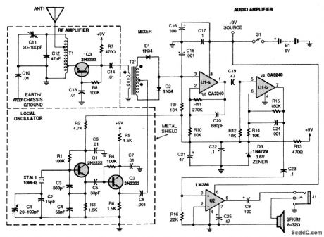
Incoming RF is picked by the antenna (ANTI) and is coupled via an autotransformer to a grounded-base amplifier (Q3) before being applied to a diode-mixer network that comprises T2, D1, and D2. The best mixer performance is obtained when both secondary windings of T2 are identical, and D1 and D2 are matched. The output of the local oscillator (LO)-a grounded-collector Colpitts oscillator (built around Q1)-is applied to emitter-follower/buffer Q2, which provides a low-impedance drive signal for the mixer. The demodulated signal is coupled to a pair of high-gain op-amp stages (U1-a and U1-b). The op amps provide a 50-dB gain. Amplifier U2 provides a 20-dB gain, thereby producing sufficient output drive for an 8-Ω speaker or 32-Ω headphones. The volume is controlled merely by adjusting the length of the whip antenna. When driving 32-Ω headphones, the circuit consumes less than 25 mA; however, the current drain increases to 40 mA when driving an 8-Ω speaker. (View)
View full Circuit Diagram | Comments | Reading(1216)
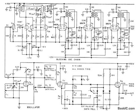
SSB_COHERENT_RADAR_OSCILLATOR
Published:2009/7/17 3:07:00 Author:Jessie

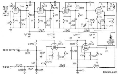
Phase information of each transmitted pulse is stored in coherent oscillator V3 for use as reference voltage for analyzing doppler return from targets. Other stages are amplifiers. Oscillator lank is L1-C1-C2. This oscillator has good free-running stability and is easily locked in phase with 30.Mc input pulse.-J. B. Theiss, More Target Data with Sideband Coherent Radar, Electronics, 36:3, p 40-43. (View)
View full Circuit Diagram | Comments | Reading(1084)
TRANSlSTOR_TESTlNG_OSClLLATOR
Published:2009/7/11 1:41:00 Author:May

With any good general-purpose transistor, circuit delivers steady AF tone to earphone. To test another transistor, substitute it in appropriate socket. No tone means it is bad. Low tone or chirp indicates questionable condition. If type (PNP or NPN) is unknown, try in both sockets. If leads of unknown cannot be identified, try all three possible positions in socket.-Circuits, 73 Magazine, July 1977, p 35. (View)
View full Circuit Diagram | Comments | Reading(763)
MEGAPULSE_GENERATOR
Published:2009/7/11 1:36:00 Author:May
Provides up to 18-Mc pulses for dynamic testing of high-speed digital computers. Can be used as clocking system. Major frequency changes in self-biased Hartley osdllcnor V6 are made with plug-in coilsll,and changes with C4.Positive output pulses,continuously variable between 0 and 20v,are generated in four output channels,in 10-microses or with 0 to 10 microsec blanks between strings of pulses when gated by pulse generator.-RW.Buchanan and B.Kautz,Dynamic Testing of Computer Building Block,Electronics,32:33,p66-68. (View)
View full Circuit Diagram | Comments | Reading(995)
WWV_RECEIVER
Published:2009/7/17 3:03:00 Author:Jessie
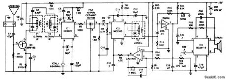
This receiver is a crystal-controlled superheterodyne receiver with an MPF102 RE amplifier, NE602 mixer, ceramic IF filter, MC1350P IF amplifier, ZN414 AM detector, and MC34119 audio output. The AGC system uses a CA3140E op amp. A 9545-kHz crystal is used in the LO. (View)
View full Circuit Diagram | Comments | Reading(7)
One_shot_multivibrator_using_an_ECG955M_timer_oscillator_chip
Published:2009/7/17 4:09:00 Author:Jessie
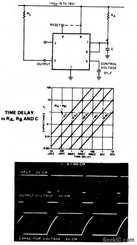
One-shot multivibrator using an ECG955M timer/oscillator chip. Upon application of a negative trigger to pin 2 the flip-flop is set, which releases the short circuit across the external capacitor. This dives the output high. The photo shows the actual waveforms generated in this mode. The time that the output is high is given by t= 1.1 RA C and can be easily determined by the graph showing time delay. Applying a negative pulse to reset terminal 4 cluing the timing cycle discharges the capacitor and causes the cycle to start again. When the reset function is not used it is recommended that it be connected to supply voltage to avoid false triggering (courtesy GTE Sylvania Incorporated). (View)
View full Circuit Diagram | Comments | Reading(940)
Ionization_chamber_smoke_detector_using_discrete_transistors_for_alarm_oscillators
Published:2009/7/17 4:01:00 Author:Jessie
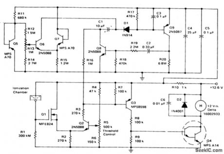
Ionization-chamber smoke detector using discrete transistors for alarm oscillators(Courtesy Motorola Semiconductor Products Inc.). (View)
View full Circuit Diagram | Comments | Reading(1300)
Pulse_width_modulator
Published:2009/7/17 3:56:00 Author:Jessie
This circuit uses both sections of an XR-13600 (Fig. 11-1B) to form a pulse-width modulator. EXAR corporation Databook 1990 p 5-258 (View)
View full Circuit Diagram | Comments | Reading(0)
25_NSEC_O5_AMP_CLOCK_PULSE_GENERATOR
Published:2009/7/10 23:53:00 Author:May
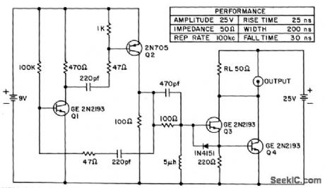


Used in computer circuits to set timing for array of circuits.Mvbr Q1-Q2 triggers pulse generator Q3-Q4.- Transistoy Manual, Seventh Edition, General Electric Co, 1964, p202. (View)
View full Circuit Diagram | Comments | Reading(641)
MODEL_TRAIN_TRACK_CONTROL_SIGNAL
Published:2009/7/17 3:47:00 Author:Jessie
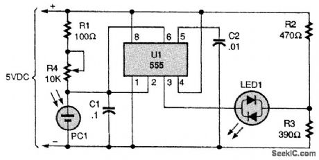
The circuit is based on a 555 timer IC, U1, and operates on 5-Vdc to make it usable with digital logic. The operating power of the circuit can be converted to 12 V by increasing the values of R2 and R3. Train detection is accomplished by photocell PC1, which should be mounted between the rails, flush with or slightly below the ties. A small light must be mounted directly above PC1 when it is used in a dark area. Resistor R4 is adjusted so that when a train covers PC1, the circuit triggers. Resistor R1 reduces the current to U1 if R4 is set for minimum resistance. Variable resistor R4 can also be ad-justed so that each individual car in a train will change the colors of LED1, a bicolor unit, back and forth, indicating train movement. That can be handy if two circuits are used, one at each end of the track block. It will indicate that the train has begun to move, Mount LED1 on the control panel. The circuit is designed to indicate a green when no train is present. When a train covers PC1, U1 switches LED1 to red, indicating that the train is in position. (View)
View full Circuit Diagram | Comments | Reading(1556)
TIME_MARK_GENERATOR
Published:2009/7/10 22:22:00 Author:May
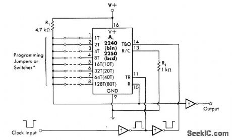
Produces precisely spaced output pulses suitable for calibrating CRO time bases. Can be programmed in binary by using 2240 for A, or in BCD by using 2250.Use crystal oscillator or other high-accuracy source for external clock, Time interval of output pulse is equal to clock width multiplied by n + 1, where n is number programmed into A, (1 to 255 for 2240 and 1 to 99 for 2250). Circuit can be programmed electronically by microprocessor if desired.-W. G. Jung, IC Timer Cookbook, Howard W. Sams, Indianapolis, IN, 1977, p218-220. (View)
View full Circuit Diagram | Comments | Reading(1473)
CAVE_MAPPING_RECEIVER
Published:2009/7/17 4:29:00 Author:Jessie
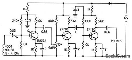
Pickup loop feeds low-noise transistor Q1, followed by twostage audio amplifier. Since low-frequency magnetic field (2 kc) is attenuated very little by rock, soil, or water, strength of received signal from transmitter in cave being mapped can be measured. When system is calibrated for distance on surface, depth can be measured.-E. R. Roeschlein, Mapping Caves Magnetically, Electronics, 33:39, p 61. (View)
View full Circuit Diagram | Comments | Reading(991)
Norton_square_wave_oscillator
Published:2009/7/17 4:26:00 Author:Jessie
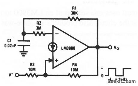
This circuit uses one section of an LM3900 to form a square-wave oscillator (with a 1-kHz output using the values shown). National Semiconductor Linear Applications Handbook 1991 p 232 (View)
View full Circuit Diagram | Comments | Reading(932)
Norton_sine_wave_oscillator
Published:2009/7/17 4:26:00 Author:Jessie
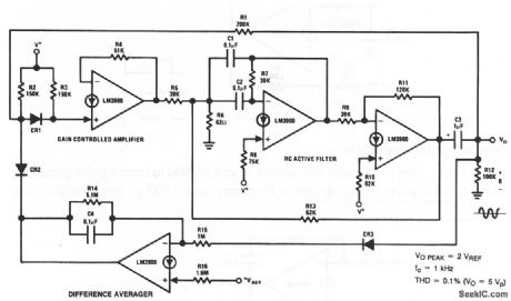
This circuit uses four sections of an LM3900 to form a sine-wave oscillator. One section is used as a gain-controlled amplifier (to sustain feedback), and another section is a difference averager that maintains a constant output level.The remaining sections are connected as an RC active filter (to produce a 1-kHz output with the values shown). National Semiconductor Linear Applications Handbook 1991 p 231 (View)
View full Circuit Diagram | Comments | Reading(1154)
Frequency_doubler
Published:2009/7/17 4:20:00 Author:Jessie
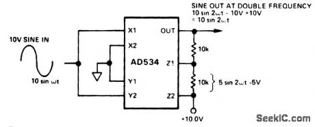
Frequency doubler. This circuit accepts a sinusoidal signal with a 10-voh amplitude and produces a double-frequency signal also having a 10-volt amplitude with no DC offset (courtesy Analog Devices, Inc.). (View)
View full Circuit Diagram | Comments | Reading(0)
| Pages:77/195 At 206162636465666768697071727374757677787980Under 20 |
Circuit Categories
power supply circuit
Amplifier Circuit
Basic Circuit
LED and Light Circuit
Sensor Circuit
Signal Processing
Electrical Equipment Circuit
Control Circuit
Remote Control Circuit
A/D-D/A Converter Circuit
Audio Circuit
Measuring and Test Circuit
Communication Circuit
Computer-Related Circuit
555 Circuit
Automotive Circuit
Repairing Circuit