
Signal Processing
Index 64
DUAL_LINE_RECEIVER_FOR_COAX
Published:2009/7/15 4:15:00 Author:Jessie
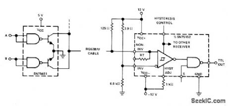
Single Texas Instruments SN75152 IC contains two receiver sections, each taking input from separate coax. Other receiver section (not shown) is identical and provides similar TTL output for its coax. Driver shown has OR capability for feeding single coax, Receiver has adjustable noise immunity and continuously adjustable hysteresis control (not shown).- The Linear and Interface Circuits Data Book for Design Engineers, Texas Instruments, Dallas, TX, 1973, p 8-78. (View)
View full Circuit Diagram | Comments | Reading(1261)
21_2125_MHz_with_VFO
Published:2009/7/14 3:50:00 Author:May
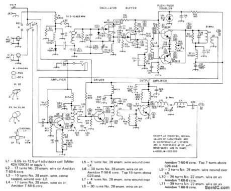
Developed for low-power CW work in 15-meter amateur band. Colpitts oscillator Q1 runs continuously at 10.5-10.625 MHz during transmit and receive, for good frequency stability, so VF0 frequency must be shifted away from operating frequency during receive periods. Supply is 12 V at 1.3 A. C6 is 4-53.5 pF. RFC4 is 16turns No. 28 enamel, RFC5 is 11 turns No. 22, and RFC6 is 6 turns No. 22, each on Amidon FT-50-61 core. Article covers construction and tune-up.-J. Rusgrove, A 15-Meter Goober Whistle, QST, Jan. 1976, p 16-19. (View)
View full Circuit Diagram | Comments | Reading(1020)
80_METER_VFO
Published:2009/7/14 3:42:00 Author:May
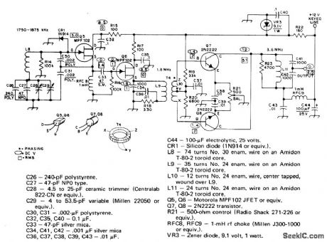
Used in place of crystal-con- trolled oscillator in low-power (QRP) amateur -transmitter. Tuning range is 1750-1875 kHz in 160-meter band. Colpitts oscillator uses JFET Q5 with series-tuned tank for good stability. Q6 provides isolation between oscillator and push-push class C doubler amplifier stage. Doubling gives desired 80-meter output.-D. DeMaw and J. Rusgrove, Learning to Work with Semicon-ductors, QST, Oct. 1975, p 38-42. (View)
View full Circuit Diagram | Comments | Reading(2444)
ORGAN_PEDAL_GENERATOR
Published:2009/7/14 3:42:00 Author:May
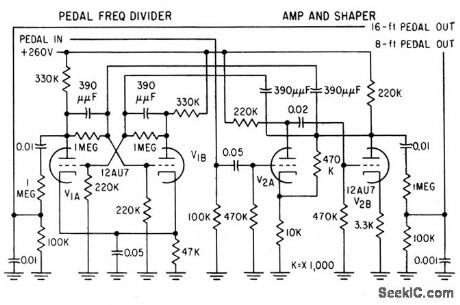
Shaper V2 yields sawtooth wave with steeper flyback than from neon oscillator. Output of V2 feeds bistable mvbr V1 which changes state with each input trigger. Bistable output at V1A is half the input frequency (one octave lower), so 16-ft pedal tones are produced without low-frequency divider stage for each tone generator.-R. H. Dorf, Electronic Organ Uses Neon Tone Generators, Electronics, 31:35, p 36-41. (View)
View full Circuit Diagram | Comments | Reading(932)
NEON_TONE_GENERATOR
Published:2009/7/14 3:41:00 Author:May

Each of 12 organ tone generators has four pairs of neon tubes in series, each pair shunted by two series capacitors. With signal taken from common point between capacitors, sufficient insolation exists to prevent feedback and spurious tones in output. Master oscillator provides initial sync for neon-lamp divider chain. Article gives capacitor values for each musical note.-R. H. Dorf, Electronic Organ Uses Neon Tone Generators, Electronics, 31:35, p 36-41. (View)
View full Circuit Diagram | Comments | Reading(1293)
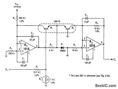
VOLTAGE_CONTROLLED_0_1_KC_OSCILLATOR__
Published:2009/7/15 20:51:00 Author:Jessie
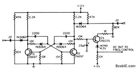
Pulse-counting discriminator in feedback loop gives adequate linearity for computing applications. As input voltage rises from 0 to 10 mV, oscillator output frequency rises proportionally.-N. W. Bell and V. Chiunti, Voltage-Controlled Oscillator Uses Negative Feedback,Electronics.35:11,p65-65. (View)
View full Circuit Diagram | Comments | Reading(921)
RANDOM_NUMBER_GENERATOR
Published:2009/7/14 3:30:00 Author:May
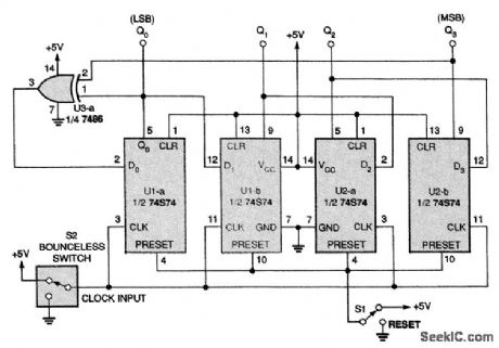
The 74574 flip-flops shown in the circuit are arranged to form a 4-bit shift register. Binary data enter the D0 input on U1-a and are sequentially shifted to each output (Q0, Q1, Q2, Q3) with each clock pulse. The data input to the shift register come from the output of U3-a, one gate of a 7486.That exclusive-OR gate compares two of the output bits from the shift register. If the two bits are the same, then the output of U3-a is 0 Y (or low). If the two bits are different, then the output of U3-a is +5 V (or high). Therefore, U3-a acts as a type of logical-feedback network that changes the data at D0, which, in turn, changes the outputs of the flip-flops. The effect of that network is to create a pseudo-random sequence of bits at the outputs of U1 and U2. (View)
View full Circuit Diagram | Comments | Reading(3301)
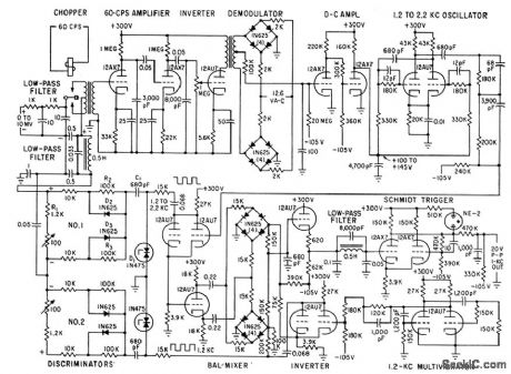
INDUCTION_HEATER_POWER_OSCILLATOR
Published:2009/7/14 3:30:00 Author:May
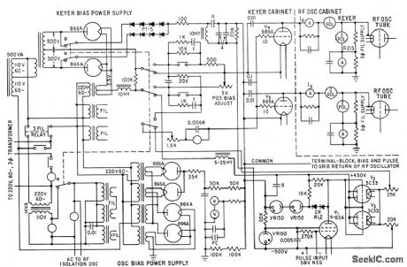
Circuit includes power supplies for oscillator and keyer bias.-R. E. Mathews and F. R.Sias, Jr., Testing Space Craft with Induction Heaters, Electronics, 35:34. P,38-41. (View)
View full Circuit Diagram | Comments | Reading(3152)
DIFFERENTIAL_AC_SIGNALS
Published:2009/7/15 20:26:00 Author:Jessie
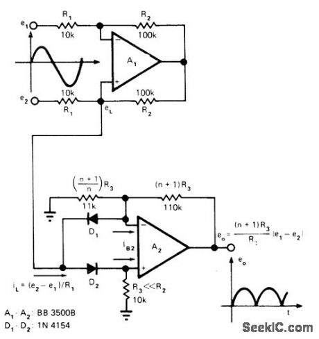
Precision full-wave rectification of differential voltage is achieved by transforming to current for rectification and reconversion to output voltage. One opamp serves as voltage-to-current converter and the other as rectifying current-to-current converter. Circuit is suitable for applications in which lower input impedance and lower frequency response are acceptable. Article gives design equations.-J. Graeme, Measure Differential AC Signals Easily with Precision Rectifiers,. EDN Magazine, Jan, 20, 1975, p 45-48. (View)
View full Circuit Diagram | Comments | Reading(2404)
SAWTOOTH_SYNC_GENERATOR
Published:2009/7/14 3:28:00 Author:May

Provides sync and sawtooth signals for power oscillator control system of induction heater.-R.E. Mathews and E.R. Sias, Jr. , Testing Space Craft with Induction Heaters, Electronics, 35:34. P,38-41. (View)
View full Circuit Diagram | Comments | Reading(1064)
DIGITAL_BURST_GENERATOR_
Published:2009/7/14 3:25:00 Author:May

Figure 1 illustrates the transmitted signal and the continuous sine wave from which it is derived. Because the HA4600 buffer has an enable/disable feature, it will pass or reject the input waveform, depending on the state of the enable pin (Fig. 2.). The input signal also is present at the input to the HFA3046 transistor array, which has been configured as a high-speed, high-gain comparator. The comparator squares up the input signal and applies it to the inputs of the two counters, X and Y. The X counter controls the buffer enable, and it determines how many cycles of the input waveform get passed to the output. The four switches SX0 through SX3 are binary-coded. Consequently, if two switches (SX0=1 cycle and SX3=2 cycles) are closed, three cycles of the input sine wave will be passed to the output. Furthermore, the input signal is connected to the Y counter, which controls the repetition rate by determining the OFF period between pulse bursts. The four switches SY0 through SY3 are binary-coded. When all of these switches are closed, the OFF period will be 16 times the period of the input waveform. With the X and Y counters set as described earlier, the repetition rate is the reciprocal of (16+3) times the period of the incoming waveform. If a longer repetition rate is desired, a flip-flop or another counter can be added in series with the output of the Y counter to extend the OFF time. R6, R7, and R8 bias the long-tailed transistor at 10 mA, which is the optimum point for speed. R5 and R6 are small enough to discharge quickly, thus preventing saturation. Configured as shown, the circuit will handle 10-MHz input signals with little degradation. The limit on frequency response is the speed of the logic and the comparator delay time. The comparator delay time can be eliminated by one-shotting out the delay. (View)
View full Circuit Diagram | Comments | Reading(1651)
ISOLATION_OSCILLATOR
Published:2009/7/14 3:25:00 Author:May
Used to isolate duty-cycle generator induction heater control system from pulser of power oscillator.-R.E.Mathews and F. R. Siad, Jr., Testing Space Craft with Induction Heaters,Electronics,35:34,p 38-41. (View)
View full Circuit Diagram | Comments | Reading(975)
ANTILOG_GENERATOR
Published:2009/7/14 3:16:00 Author:May
Basic log generator circuit is rearranged to pelform inverse operation of antilog (exponential) generation. Exponential current generated by O2 is summed at current-to-voltage converter A2.Q1 voltage drive to Q2 is such that collector cument ofQ2 is exponentially related to voltage at base of Q1.Temperature-compensating divider scales input sensitivity to 1V per decade. Feed-forward connections at A1 andA2 optimize circuit for speed.-W. G. Jung, IC 0p-Amp Cookbook, Howard W. Sams, Indianapolis, IN, 1974, p 214-216. ' (View)
View full Circuit Diagram | Comments | Reading(2373)
THREE_TONE_GENERATOR
Published:2009/7/14 3:10:00 Author:May
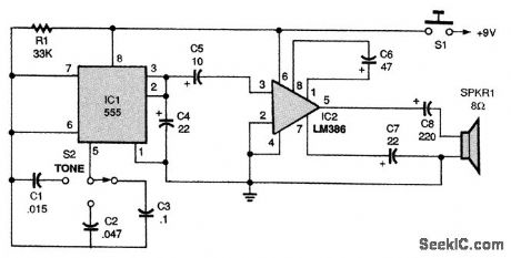
The three-tone generator makes a great warning device. It has a lot of uses; for example, if the appropriate switch is used for S1, the circuit can be used as a burglar alarm. When S1 is pressed, it turns on the circuit. The tone frequencies depend on resistor R1 and capacitors C1 through C3.Switch S2 lets you select between those capacitors. Capacitor C1 produces the highest frequency because it has the lowest capacitance, while C3 generates the lowest frequency. (View)
View full Circuit Diagram | Comments | Reading(1124)
SIMPLE_WIDEBAND_NOISE_GENERATOR
Published:2009/7/14 3:03:00 Author:May

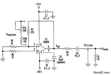
This relatively simple op-amp noise generator amplifies the input voltage noise of a wideband, decompensated op amp. If a device with a single-gain stage is selected, the output noise will be spectrally flat up to the closed-loop bandwidth. The op amp is manufactured by Analog Devices Inc. (View)
View full Circuit Diagram | Comments | Reading(1686)
RESET_GENERATOR
Published:2009/7/14 2:57:00 Author:May

This VCC monitor circuit draws less than 10μA,yet it can generate reliable RESET signals.
Very low quiescent current makes the reset generator shown suitable for use with microcontrollers that spend most of their time in the “sleep” mode .The system’s power Source,a charged 0.047-μF “Supercap” capacitor(C1),can go without a recharge for intervals exceeding24 hours .The allowable supply-voltage range for the reset circuit is 2 to 11 V. R1 and R2 make it possible to set the switching threshold as low as 1.2 V (the values shown provide a 4.10-V threshold). Hysteresis introduced by R3 minimizes the effect of reference noise and external EMI . Using the values gtven for R2 and R3 (1 MΩ and 10 MΩ),the switching threshold (Vt) is obtained by adjusting the value of R1 alone∶R1 (in megohms)=0.770Vt-0.910. External connections tie the internal reference voltage tothe inverting input of each comparator. Comparator A monitors the supply voltage .When this voltage dips below the threshold established by R1 and R2,the comparator output initiates a RESET pulse via D3 and discharges the timing capacitor (C3)via diode D1. Comparator B determines the pulse duration with help from the time-delay components R4 and C3.Because the duration (approximately 250 ms) is well above the 5-ms mlnlmum required in this case,the effect of supply voltage on pulse width call be ignored . D2 allows the circuit to respond to short outages by providing another quick-discharge path for the timing capacitor. Comparator C is a spare that supplies a complementary output or low-line warnlng. Comparator D acts as an active AND gate for logic-high signals from comparators A and B . The pull-up resistor in many such circuits is 100 kΩ or less (to avoid errors caused by the comparator’s input leakage). In this particular case,it would provide a path for excessive battery discharge during reset. (View)
View full Circuit Diagram | Comments | Reading(937)
AF_RECTANGULAR_WAVE
Published:2009/7/15 5:17:00 Author:Jessie
Frequency can be adjusted over wide AF range, with ON and OFF times of rectangular output signal independently varied between 35 and 60% on by choice of values for C1 (0.05to 40 μF), R2 (1K or 2K), and R3 (7.3K to 27K). Minimum value of R3 is 6K.-D.E. Manners, Adjustable Rectangular-Wave Oscillator Interfaces with IC Logic, EDN|EEE Magazine, Sept. 15, 1971, p 46. (View)
View full Circuit Diagram | Comments | Reading(751)
DIFFERENTIAL_D_C_AMPLIFIER_CONTROLS_23O_KC_C_W_RADAR_OSCILLATOR
Published:2009/7/15 5:06:00 Author:Jessie
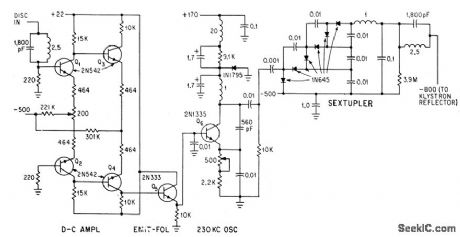
Combined output of two detectors in dual-mode cavity, having typical discriminator S curve, is amp lified by four transistors in differential d-c circuit and applied to oscillator through emitter-follower to make output voltage swing up to 20%. Voltage sextupler applies step-up voltage to reflector of klystron, to maintain klystron frequency constant within 0.2 Mc.-H. D. Raynes, C-W Radar Measures Artillery Ballistics, Electronics, 37:1, p 31-33. (View)
View full Circuit Diagram | Comments | Reading(934)
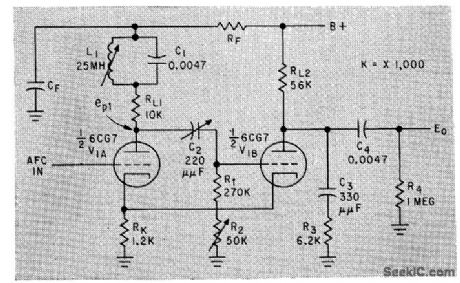
TV_HORIZONTAL_SWEEP_OSCILLATOR
Published:2009/7/15 5:05:00 Author:Jessie
Cathode-couped multivibrator includes noise-immunizing tuned circuit in plate circuit of 'triode.-C. L. Barsony, Graphical Checkout of Multivibrator Design, Electronics, 33:8, p 55-57. (View)
View full Circuit Diagram | Comments | Reading(1276)
VIDEO_SIGNAL_PROCESSOR
Published:2009/7/15 23:12:00 Author:Jessie
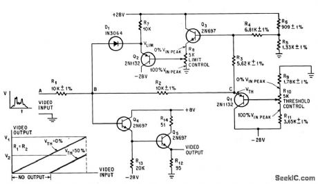
R10 adjusts threshold level and R8 adjusts limit level between which video input signal will be fed to crt display.-A. E. Popodi, Reliable Repertoire Of Display Circuits, Electronics, 38:2, p 60-66. (View)
View full Circuit Diagram | Comments | Reading(800)
| Pages:64/195 At 206162636465666768697071727374757677787980Under 20 |
Circuit Categories
power supply circuit
Amplifier Circuit
Basic Circuit
LED and Light Circuit
Sensor Circuit
Signal Processing
Electrical Equipment Circuit
Control Circuit
Remote Control Circuit
A/D-D/A Converter Circuit
Audio Circuit
Measuring and Test Circuit
Communication Circuit
Computer-Related Circuit
555 Circuit
Automotive Circuit
Repairing Circuit