
Signal Processing
Index 75
RAMP_GENERATOR_DRIVES_TRlGGER
Published:2009/7/19 21:39:00 Author:Jessie
Circuit is relaxation oscillator providing short, fast pulses for triggering mvbr. Upper operating frequency is about 1 Mc for values shown. Efficiency is high yet total component cost is under $2.-C. F. Andren, High Efficiency Relaxation Oscillator, EEE, 14:4, p 43. (View)
View full Circuit Diagram | Comments | Reading(949)
TOUCH_OPERATED_CODE_PRACTICE_OSCILLATOR
Published:2009/7/12 20:43:00 Author:May
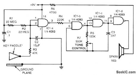
A touch-operated CPO is shown in the figure. The gates of IC1-a are biased high through the two 22-MΩ resistors (R1 and R2), keeping its output low. Gates IC1-b and IC1-c are connected in an audio oscillator circuit that can operate only when pin 5 of IC1-b is high. The last gate of the 4093, IC1-d, adds isolation to the oscillator's circuit and drives the speaker (SPKR1). Touching the key paddle and ground plane lowers IC1-a's input gate voltage to near zero, allowing the output at pin 3 to go high. The tone generator then turns on and sends out an audio note. The touch key paddle and ground plane can be made from a circuit board or any other conductible material. Note that the ground plane should lie flat for a hand rest and the key paddle should be positioned for ease of touch. (View)
View full Circuit Diagram | Comments | Reading(998)
PLL_CODE_PRACTICE_OSCILLATOR
Published:2009/7/12 20:41:00 Author:May
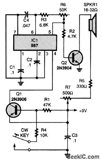
This CPO usesa 567 phase-locked loop, IC1, as the variable tone generator. The oscillator's frequency is set by R6, and the frequency range can be changed by selecting a different-value capacitor for C5. To lower the oscillator's frequency range, make the value of C5 larger, and to increase the frequency range, reduce C5. A general-purpose 2N3906 PNP transistor, Q1, supplies power to the 567 through pin 4 each time that the CW key is closed. Meanwhile, Q2, a general-purpose 2N3904 NPN transistor, buffers the oscillator's output and drives the speaker. Potentiometer R7 sets the output volume. (View)
View full Circuit Diagram | Comments | Reading(1179)
MORSE_CODE_OSCILLATOR
Published:2009/7/12 20:38:00 Author:May
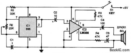
The circuit is built around a 555 oscillator (IC1) and an LM386 audio amplifier (IC2). The 555 circuit is an astable oscillator, with the chip output retriggering the circuit. When the key (S1) is pressed, it activates the circuit. The 555 oscillates at a frequency determined by R1, R2, and C1. Potentiometer R2 is used to adjust the tone frequency of the oscillator. Some of the output current of IC1 is coupled to IC2 via a 10-°F capacitor, C2, so that it will be sufficient to drive a loudspeaker. Because the circuit has no gain control, the volume depends on the size and wattage of the speaker. (View)
View full Circuit Diagram | Comments | Reading(2498)
SHORT_WAVE_RECEIVER
Published:2009/7/17 2:32:00 Author:Jessie

Using a Signetics NE602 in a varactor-tuned front end, the circuit of a shortwave receiver can be very simple and yet give high performance. This circuit also uses a ceramic filter as a sensitivity-determining device, two IF stages, AGO, and an audio amplifier. It has a sensitivity of under 1μV. The table shows coil data for the frequencies from 5 to 16 MHz. The values C18, C19, and C23 depend on the frequency range chosen. (View)
View full Circuit Diagram | Comments | Reading(4037)
TRF_RADIO
Published:2009/7/17 2:29:00 Author:Jessie
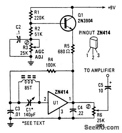
This simple AM radio uses a Ferranti ZN414 IC and runs from a 9-V supply. A 5/16 -diameter ferrite rod serves as an antenna, and uses about 85 turns of #28 enatnelled wire. (View)
View full Circuit Diagram | Comments | Reading(2640)
REFLEX_RADIO_RECEIVER
Published:2009/7/17 2:28:00 Author:Jessie
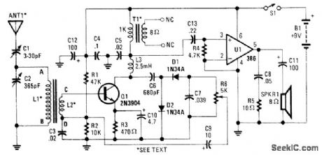
The RF signal is passed from the antenna through C1 to the tuned circuit made up of L1 and C2.Oneend of L2 feeds the RF signal to the base of Q1 for amplification and the other end ties to the junction ofR1and R2 to supply bias to the transistor.A 0.02-μF capaotor,C3,places the“D”end of L1 at RE ground.
The amplified RF signal is fed through C6 to a two-diode doubler/rectifier circuit and then on to thevolume control,R6.The wtper of R6 feeds the detected audio signal through C9 to the junction of R1,R2,and the“D”end of u.The“D”end of L2 is at RF ground,but not AF ground,allowing the AF signal tobe passed through L2 to the base of Q1 for amplification. The junction of the 2.5-mH choke and T1 is placed at RF ground through C5. The amplified audio is fed from this junction to the mput ofthe 386 audioamplifier,U1,to drive the 4 8-Ω speaker.The single transistor has performed a dual duty by amplifying the RF and AM signals at the same time. (View)
View full Circuit Diagram | Comments | Reading(3380)
SIMPLE_LOW_FREQUENCY_RECEIVER
Published:2009/7/17 2:26:00 Author:Jessie
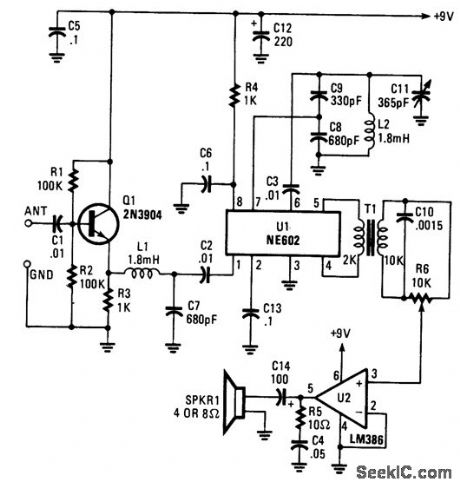
Using an NE602 heterodyne detector and U1 as an RF amplifier, this receiver tunes the middle portion of the low-frequency spectrum from 150 to 250 kHz. U2 is a loudspeaker amplifier. (View)
View full Circuit Diagram | Comments | Reading(2637)
35_TO_10_MHz_SIMPLE_SUPERHETERODYNE_RECEIVER
Published:2009/7/17 2:25:00 Author:Jessie

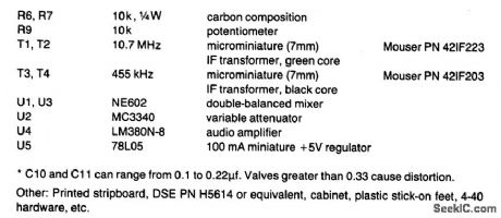
In this circuit,U1 is a frequency converter that feeds the 455-kHz IF stage U2 and detector U3. U4 is the audio output stage. R9 is a gam control that vanes the gam of U2.Coil dataisgtven h the part list. (View)
View full Circuit Diagram | Comments | Reading(5702)
PULSE_STRETCHER
Published:2009/7/17 1:48:00 Author:Jessie
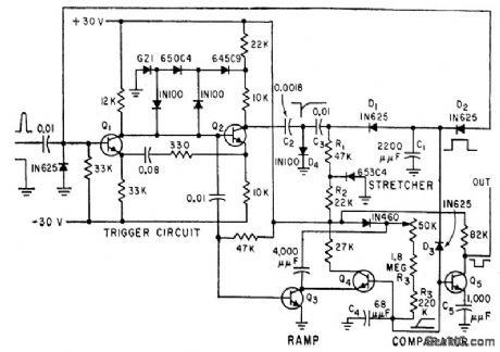
Used where low-amplitude pulses must be converted to time in. formation. Output is used to control oscillator.-D. N. Carson and S. K. Dhawan, Data Conversion Circuits for Earth Satellite Telemetry, Electronics, 33:3, p 82-84. (View)
View full Circuit Diagram | Comments | Reading(0)
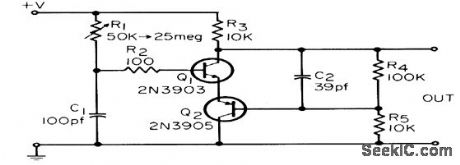
PRACTICE_OSCILLATOR
Published:2009/7/11 5:04:00 Author:May

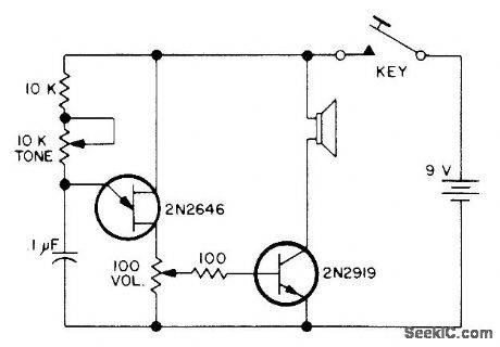
Simple design provides for adjustment of both volume and tone.-Circuits, 73 Magazine, July 1974, p 81. (View)
View full Circuit Diagram | Comments | Reading(943)
HIGH_VOLTAGE_NEGATIVE_ION_GENERATOR
Published:2009/7/11 4:49:00 Author:May
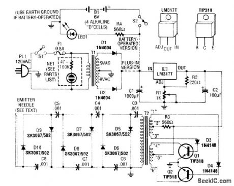
A modified B/W TV flyback transformer is used in this circuit with a voltage multiplier to produce 9- to 14-kV negative voltage. This is connected to a discharge needle to produce negative ions. (View)
View full Circuit Diagram | Comments | Reading(4904)
CORONA_WIND_GENERATOR
Published:2009/7/11 4:42:00 Author:May
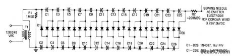
This 25-stage voltage doubler will generate corona wind. 120 Vac, or 3.75 kVdc when powered from 240 Vac.or 7.5 kvdc when powered 240 Vac (View)
View full Circuit Diagram | Comments | Reading(1711)
STABILIZED_LOW_FREQUENCY_OSCILLATOR
Published:2009/7/11 4:36:00 Author:May
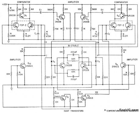
Transistors Q1 and Q4 compare charging voltages of mvbr timing capacitors C1 and C2 to fixed reference voltage.When a capacitor voltage is greater than reference.its comparator switches its bistablw mvbr to opposite state,so capacitor is discharged by dump transistor.Arrangement makes output frequency essentially independent of temperqture from-25℃ to+75℃.for frequency range of 0.01 to 100,000 cps,-J.D.Long.Novel Differential Amplifier Stabilizes Multivibrator,Electronics,35:24,p53-54 (View)
View full Circuit Diagram | Comments | Reading(870)
VCO
Published:2009/7/11 4:31:00 Author:May

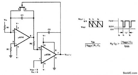
Q1. an FET. is used as a variable resistance to control frequency of oscillator. (View)
View full Circuit Diagram | Comments | Reading(0)
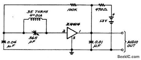
VARACTORLESS_VCO
Published:2009/7/11 4:28:00 Author:May
The varactorless VCO utilizes a modifted Clapp-oscillator conftguration, together with some data on the type of transistor, circuit values, and operating frequencies. (View)
View full Circuit Diagram | Comments | Reading(965)
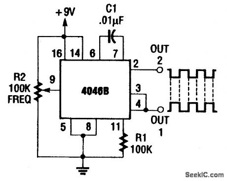
WIDE_RANGE_VCO
Published:2009/7/11 4:24:00 Author:May
This circuit covers 0 to 1.4 kHz.C1 can be changed to cover other ranges,as desired. (View)
View full Circuit Diagram | Comments | Reading(1213)
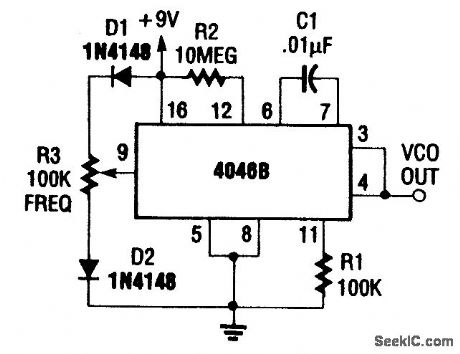
BIPHASE_WIDE-RANGE_VCO
Published:2009/7/11 4:21:00 Author:May
Using a CD4046B, this circuit generates abiphase signal.The frequency range is below 100Hz to about 1.5 kHz. (View)
View full Circuit Diagram | Comments | Reading(2050)
ONE_CHIP_AM_RADIO
Published:2009/7/17 3:01:00 Author:Jessie
The ZN414 IC contains a complete AM radio, with AGC, except for an audio section. Like an MMIC, it is powered through its output terminal. (View)
View full Circuit Diagram | Comments | Reading(800)
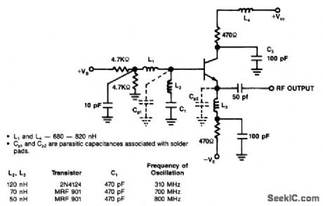
_VOLTAGE_TUNED_VHF_OSCILLATOR
Published:2009/7/11 4:08:00 Author:May
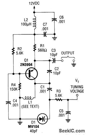
This VHF VCO circuit is suitable for 30 to 200 MHz. Q1 can be replaced by a 2N3563 for operation above 100 MHz. L1 is chosen to resonate to the desired frequency with the varactor capacitance of 40 pF. Other vatactors can be substituted or two back-to-back vat-actors can be used for better linearity, depending on the application. (View)
View full Circuit Diagram | Comments | Reading(2588)
| Pages:75/195 At 206162636465666768697071727374757677787980Under 20 |
Circuit Categories
power supply circuit
Amplifier Circuit
Basic Circuit
LED and Light Circuit
Sensor Circuit
Signal Processing
Electrical Equipment Circuit
Control Circuit
Remote Control Circuit
A/D-D/A Converter Circuit
Audio Circuit
Measuring and Test Circuit
Communication Circuit
Computer-Related Circuit
555 Circuit
Automotive Circuit
Repairing Circuit