
Signal Processing
Index 70
WWV_REGENERATIVE
Published:2009/7/16 4:18:00 Author:Jessie

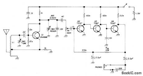
Tunes from 4.7 to 15.5 MHz, covering three WWV frequencies, 20- and 40-meter amateur bands, and several foreign broadcast bands. Draws only 1.5mA from single D cell when using headphones with 2000-ohm or higher impedance. Performs well with AM, CW, or SSB. When oscillating, detector provides own BFO signal, L1 is 3.8 μH, with emitter tap 1,turn from ground. Use clip for adjusting antenna tap. Tuning requires two hands. - C.Hall, Simple Regenerative WWV Receiver, Ham Radio, April 1973, p 42-45.
(View)
View full Circuit Diagram | Comments | Reading(1381)
PRECISION_FULL_WAVE_DIODE_DETECTOR
Published:2009/7/16 4:16:00 Author:Jessie
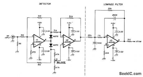
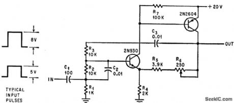
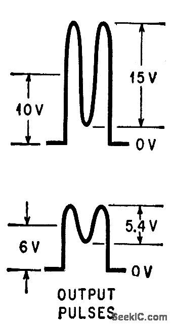
Uses opamp to reduce input voltage at which transfer curve of diode detector becomes nonlinear by factor equal to open-loop gain of opamp. Chief drawback is that delay for positive input signals, which are inverted and amplified 2 times, is twice that for composite signals. Be-VTVM cause of delay difference, signals do not subtract in phase and high-frequency performance suffers. Values shown are for test purposes, with low-pass active filter having 2-kHzcutoff.-H. Olson, Diode Detectors, Ham Radio, Jan. 1976, p 28-34. (View)
View full Circuit Diagram | Comments | Reading(1313)
9_MHz_TUNED_OUTPUT
Published:2009/7/16 4:15:00 Author:Jessie
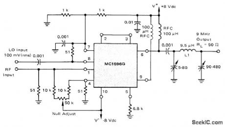
Motorola MC1596G balanced modulator connected as double-balanced mixer has 3-dB bandwidth of 450 kHz at output. Local oscillator signal LO is injected at upper input port and modulated signal of about 15 VRMS maximum at lower input port. Conversion gain is 13 dB for 30-MHz input and 39-MHz LO.-R. Hejhall, MC1596 Balanced Modulator, Motorola, Phoenix, AZ, 1975, AN-531, p7.
(View)
View full Circuit Diagram | Comments | Reading(1023)
450_MHz_PREAMP
Published:2009/7/16 4:14:00 Author:Jessie
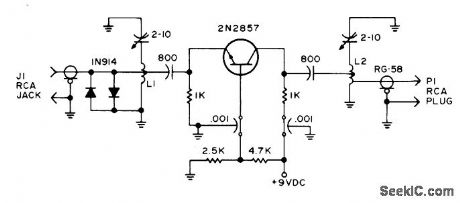
Provides up to 10-dB extra gain for older tube-type 450-MHz receivers. Gives significant improvement in receiver sensitivity and quieting. Use of trough-line inductors simplifies construction. 1N914 diodes in parallel at input jack protect transistor from burnout by nearby transmitter. L1 and L2 are made from 1/4-inch diameter copper tubing, 8.6 cm long. Article covers construction and operation.-C. Klinert, Easy Preamp for 450 MHz, 73 Magazine, May 1973, p 33 and 36-38. (View)
View full Circuit Diagram | Comments | Reading(1371)
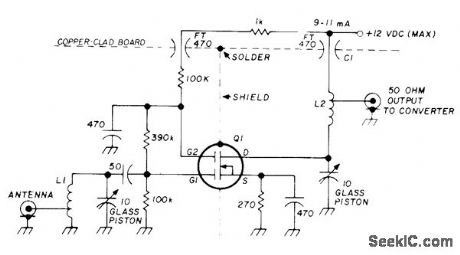
SWEPT_OSCILLATOR_FOR_HAM_BAND_ANTENNA_TUNING
Published:2009/7/13 3:39:00 Author:May
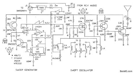
Transistor Q1 acts as a constant-current generator, charging capacitor C1 at a rate determined by the value of R1. The high input impedance of U1b ensures that the constant-current generator is not excessively loaded and forwards the voltage level of C1 to U1c. U1c is configured as a comparator, and output pin 8 goes low when pin 9 rises above 9 V. This switching action applies a trigger pulse via capacitor C2 to activate the monostable multivibrator, U2. The resulting high pulse from pin 3 of U2 provides a discharge path for capacitor C1 through turned-on transistor Q2. A continuous sweep ramp with reset is produced at pin 7 of Ulb at a rate determined by RIC1 (approximately 75 Hz). The swept oscillator section consistsof a dual-gate MOSFET transistor in a Colpitts configuration, followed by a buffer amplifier that provides the RF from the selected frequency range to an output amplifier and short antenna. As the output sawtooth waveform from U2, pin 7, is applied to the varactor, the capacitance of the tank circuit decreases from approximately 62 pF at the low end of the ramp to a very low value at the maximum sweep level of about 9.2 V. The on-off switching action of the sweep waveform modulates the generated RF to produce an obnoxious buzz, which is easy to differentiate from other low-level signals at the selected receiver frequency when adjusting the tuner or antenna.
(View)
View full Circuit Diagram | Comments | Reading(1188)
VARIABLE_SQUARE_WAVES
Published:2009/7/16 4:01:00 Author:Jessie
Output is adjustable from 0.5 cps to 60 kc at currents up to 150 ma, without appreciable corner rounding of waveform, with variable pulse width and variable interval between pulses, for driving flash lamps, relays, and computer pales.-J. D. Reed, Square Wave Generator with Variable On and Off Times, EEE, 10:10, p 27-28. (View)
View full Circuit Diagram | Comments | Reading(850)
2_METER_SINGLE_VMOS
Published:2009/7/16 4:00:00 Author:Jessie
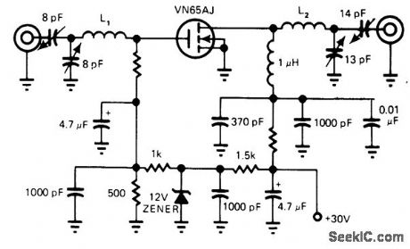
Provides 5-W PEP output at 146 MHz, with noise figure of only 2.35 dB. Developed for amateur radio applications. Uses Siliconix VN65AJ transistor. - E. Oxner, Will VMOS Power Transistors Replace Bipolars in HF Systems? , EDN Magazine, June 20, 1977, p71-75.
(View)
View full Circuit Diagram | Comments | Reading(831)
DIRECT_CONVERSION
Published:2009/7/16 7:07:00 Author:Jessie
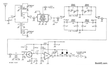
Simple direct-conversion amateur receiver uses VFO and mixer to produce AF signal directly, with no IF amplifier or second detector. For SSB reception, VFO is tuned to frequency of suppressed carrier. For CW, VFO is detuned enough to give note of desired pitch. Not suitable for AM or FM reception. Separate input tuned circuits are used for 15-40 meters and for 80-160 meters. Use ferrite or powdered iron toroid cores for coils, with turns determined experimentally. L7 and L8 are 88-mH toroids with series-connected windings. R1 is used to attenuate strong signals. Article gives circuit for VFO and buffer amplifier. Separate VFO is used for each band (160, 80, 40, 20, and 15 meters). Construction details are given, along with advantages and drawbacks of direct conversion.-D. Rollema, Direct-Conversion Receiver, Ham Radio, Nov. 1977, p 44-55. (View)
View full Circuit Diagram | Comments | Reading(1360)
PUSH_PULL_RF
Published:2009/7/16 7:06:00 Author:Jessie
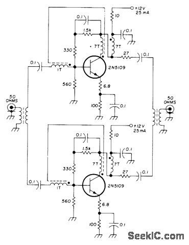
Uses VHF power transistors to obtain wide dynamic range. Transformers are trifilar wound on Indiana General F625-9-T09 toroid cores. Circuit has extremely low VSWR at both input and output, along with low noise figure. Second-order intermodulation products can be suppressed nearly 40 dB over single stage. Either RCA 2N5109 or Amperex BFR95 transistors can be used. Gain is about 11 dB.Current feedback is used through unbypassed 6.8-ohm emitter resistor, voltage feedback through unbypassed 330-ohm base-to-collector resistor, and transformer feedback through third winding on wideband transformer to stabilize input and output impedances.-U. L.Rohde, High Dynamic Range Receiver Input Stages, Ham Radio, Oct. 1975, p 26-31. (View)
View full Circuit Diagram | Comments | Reading(1284)
RF_INPUT_STAGE
Published:2009/7/16 7:01:00 Author:Jessie
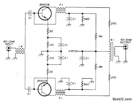
Push-pull transistorized RF stage for communication receiver uses voltage and current feedback to minimize intermodulation distortion. Transformers serve to stabilize impedance. Circuit is basically constant-current device. Second-order intermodulation distortion products are suppressed almost 40 dB more than with single-transistor stage. To apply AGC, replace the two 270-ohm resistors with single PIN-diode shunt regulator.-U. L. Rohde, Optimum Design for High-Frequency Communications Receivers, Ham Radio, Oct.1976, p 10-25. (View)
View full Circuit Diagram | Comments | Reading(2285)
STEPPING_SWITCH_PULSER
Published:2009/7/16 5:48:00 Author:Jessie
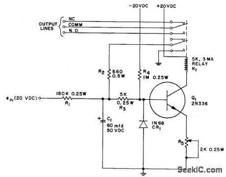
Used to advance stepping switch automatically at predetermined rate, in automatic test equipment providing go-no-go indications. C1 controls output pulse wideth to give 80-msec on time, for reliable actuation of switch that normally requires 20 millisec. Rang of off time, controlled by R5 , is 20 millisec to 7 sec.-.Wilson Step Switch Pulser, EEE, 10:11, P 26-27 . (View)
View full Circuit Diagram | Comments | Reading(790)
PULSE_CLAMP
Published:2009/7/16 5:46:00 Author:Jessie
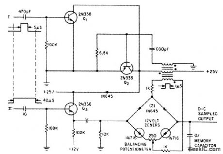
Clamps pulses in millivolt range to any d-c level even though pulses are below barrier potentials. Also used for sampling pulse amplitudes and for storing sampled amplitude in memory capacitor.-A. J. Koll, E. Bleckner, and O. C. Srygley, Semiconductor Clamp Handles Millivolt Signals, Electronics, 33:35, p 64-65. (View)
View full Circuit Diagram | Comments | Reading(867)
PULSED_OSCILLATOR
Published:2009/7/16 5:35:00 Author:Jessie
Circuit is pulsed on only when required ,as in tone generators where output is needed only occasionally and power must be conserved. Uses Wien-bridge oscillator have rang of 100 cps to 100 kc, which operates only when gating pulse is applied to input. Amplitude of output oscillations varies with amplitude of gating pulsed.-R.C. Lavigne and L. L. Kleinberg, Pulsed Oscillator Conserves Power, Electronics, 39:17, p 98-99. (View)
View full Circuit Diagram | Comments | Reading(1260)
MULTI_WAVEFORM_OSCILLATOR
Published:2009/7/16 5:31:00 Author:Jessie
By varying collector load, emitter resistors, and C, oscillator can produce triangular wave, square wave up to 30 Mc, microwattt audio signal, or serve as voltage-controlled oscillator. Values shown, with 6.v supply and 0.01 mfd mined for C, give 0.8 V peak-to-peak square wave at about 1 Mc. –P. Lefferts, Multi-Oscillator Gives Simple Waveforms, 30-Mc Output, EEE, 12:10, P 60. (View)
View full Circuit Diagram | Comments | Reading(1194)
35_4_MHz_WITH_TUNING_DIODES
Published:2009/7/16 5:28:00 Author:Jessie
Miniaturized communication receiver was developed for use as tunable IF fed by external converter for all-band coverage up to 30 MHz, Motorola MVAM-1 triple tuning diode serves in place of customary three-gang tuning capacitor. Two Murata SFD-455D ceramic filters provide IF selectivity. MFC6030 voltage regulator provides around 7 VDC with regulation required for diode tuning. Regulator also supplies VFO and BFO. Standard 3/8-in diameter 455-kHz transistor IF transformers were stripped and used for coil forms. T3 is 455-kHz IF with secondary changed to 1 turn. Remove pins 4, 6, and 8 from Silicon General SG3402T mixer.-R. Megirian, Design Ideas for Miniature Communications Receivers, Ham Radio, April 1976, p 18-25. (View)
View full Circuit Diagram | Comments | Reading(2079)
RZ_TO_NRZ_ONE_SHOT
Published:2009/7/16 5:26:00 Author:Jessie
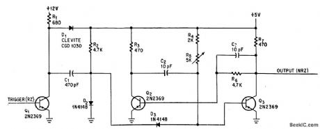
Zero recovery time of monostable multivibrator arrangement, achieved by using energy of input capacitor to recharge timing capacitor C2, makes circuit useful for converting digital data from return-to-zero format to non-return-to-zero. -P. T. Rux, One-Shot Multivibrator with Zero Recovery Time, Electronics, 39:2, p 75-76. (View)
View full Circuit Diagram | Comments | Reading(1020)
3_KC_SCR_TRIGGER
Published:2009/7/16 5:25:00 Author:Jessie
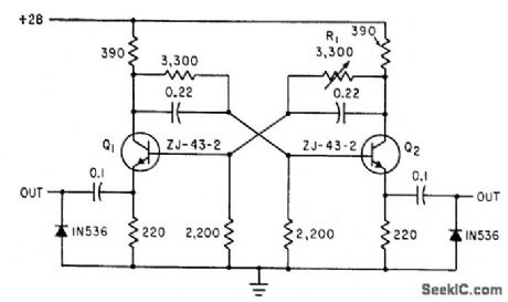
Two outputs from mvbr give alternating trigger pulses to each rectifier. R1 is adjusted for symmetrical operation.-D. V. Jones, Turn-Off Circuits for Controlled Rectifiers, Electronics, 33:32, p 52-55. (View)
View full Circuit Diagram | Comments | Reading(814)
144_MHz_PREAMP_1
Published:2009/7/16 5:25:00 Author:Jessie
Low-noise 2-meter preamp has 18-dB gain and typical noise figure of 1.7 dB. L1 and L2 are each 31/2 turns No. 18 wound 1/2 in long on 3/8-in form and tapped 1 turn from cold end. MOSFET Q1 is MEM554C, 3N159, 3N140, or 3N141. Avoid static charges until MOSFET is connected. Developed for use with tube-type 2-meter converter.- E. Noll, Circuits and Techniques, Ham Radio, April 1976, p 40-43. (View)
View full Circuit Diagram | Comments | Reading(2753)
CHOKE_CONTROLLED_FREE_RUNNING_MVBR
Published:2009/7/16 5:23:00 Author:Jessie
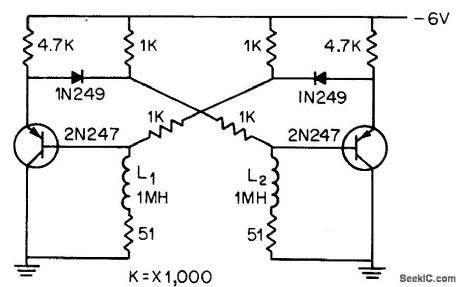
Small resistors between chokes and ground bias transistors initially into active region to insure self-starting. Crossover resistors insure that chokes recover rapidly.-W. M. Carey, Using Inductive Control in Computer Circuits, Electronics, 32:38, p 31-33. (View)
View full Circuit Diagram | Comments | Reading(865)
RELAY_ONLY_MVBR_FOR_A_C
Published:2009/7/16 5:22:00 Author:Jessie
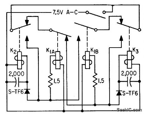
Use of a-c latching relay and rectifier diodes permits operation of low-frequency relay-type mvbr from a-c source.-R. L. Ives, Multivibrator for Low Frequencies Uses Relays, Electronics, 34:32, p 166-169. (View)
View full Circuit Diagram | Comments | Reading(889)
| Pages:70/195 At 206162636465666768697071727374757677787980Under 20 |
Circuit Categories
power supply circuit
Amplifier Circuit
Basic Circuit
LED and Light Circuit
Sensor Circuit
Signal Processing
Electrical Equipment Circuit
Control Circuit
Remote Control Circuit
A/D-D/A Converter Circuit
Audio Circuit
Measuring and Test Circuit
Communication Circuit
Computer-Related Circuit
555 Circuit
Automotive Circuit
Repairing Circuit