
Signal Processing
Index 67
STABLE_SINE_WAVE_GENERATOR
Published:2009/7/13 23:11:00 Author:May
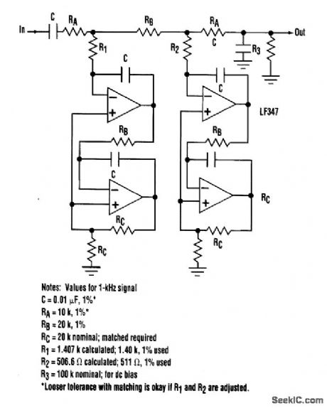
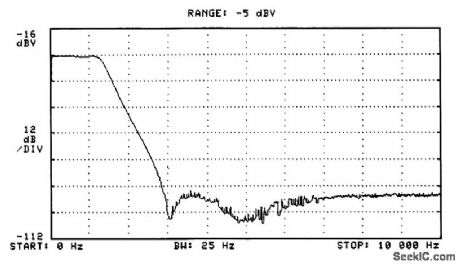
Semidigital circuits (e.g., crystal oscillators and dividers) can create square waves of very stable amplitude and frequency. Removing the odd harmonics is a reasonable task for a filter. The obvious solution, a narrowband filter, isn't acceptable because analog types are notorious for poor stability.Digital and semidigital types (e.g., switched capacitor) are better in this respect, but they add their own noise and harmonics. The task can be accomplished using the filter shown. Without R1 and R2, it is an active version of a five-pole passive low-pass LC ladder. This type has excellent amplitude stability in the passband, 30 dB/octave slope outside the passband, low component sensitivity, and a capacitor to ground at the output, which ensures continuous high-frequency rolloff and minimizes stray noise pickup. The rejection would be inadequate at the third and fifth harmonics, but notches at these frequencies can be created with just two more resistors, RI and R2. This turns the device into an elliptic-like filter. (View)
View full Circuit Diagram | Comments | Reading(1048)
SUPERREGENERATIVE
Published:2009/7/15 23:37:00 Author:Jessie
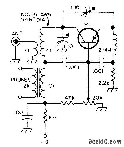
Simple single-transistor superregenerative receiver is adequate for copying many local signals in 2-meter amateur band. With components shown, tuning range is about 90 to 150 MHz. Transistor can be GE-9 or HEP-2.-Circuits, 73 Magazine, Feb. 1974, p 100. (View)
View full Circuit Diagram | Comments | Reading(2156)
VFO_WITH_DIRECT_CONVERSION_DETECTOR
Published:2009/7/15 23:34:00 Author:Jessie
Used in demodulating SSB and CW signals. Incoming signal is heterodyned with VFO output to give direct conversion to audio. Audio filter R4-C7-C8 allows only AF components to be transferred to audio amplifier Q2. Oscillator can be operated alone for other purposes by removing jumper between output terminals 2 and 3, then applying +24 V to terminal 3 and negative supply to terminal 4. Load on low-level output of oscillator has negligible effect on frequency, Load on high output may change frequency, but this can be corrected by retuning oscillator if load is constant. Values shown are for 80-meter band.-E. M. Noll, FET Principles, Experiments, and Projects, Howard W. Sams, Indianapolis, IN, 2nd Ed., 1975, p 165-173.
(View)
View full Circuit Diagram | Comments | Reading(974)
10_METER_PBEAMP
Published:2009/7/15 23:32:00 Author:Jessie
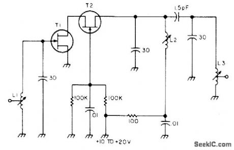
Simple preamp can also be used on 2 meters with appropriate change of coils. Needs no neutralization. Developed for use with receiver capable of receiving satellite transmissions on 29.45 to 29.55 MHz. Transistors can be MPF 102, MPF 106, or 2N4416. All coils are 1.2 μH having 7 turns No. 26 enamel on 3/16-inch slug-tuned form. L1 and L3 have tap at 3 turns. -G. L. Tater, CQ OSCAR 7, 73 Magazine, Feb. 1975, p 54-56 and 58-60. (View)
View full Circuit Diagram | Comments | Reading(799)
DUAL_GATE_MOSFET_MIXER
Published:2009/7/15 23:30:00 Author:Jessie
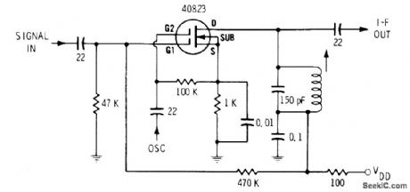
RF and oscillator signals are applied to gates G1 and G2 for mixing in MOSFET. Choice of sum or difference frequency is determined by values used in tank circuit and by tuned circuits of IF amplifier.-E.M. Noll,″ FET Principles, Experiments, and Projects,″ Howard W. Sams, Indianapolis, IN, 2nd Ed., 1975,p 141-142. (View)
View full Circuit Diagram | Comments | Reading(2293)
ONE_FILTER_THREE_PHASE_SINE_WAVE_GENERATOR
Published:2009/7/13 22:57:00 Author:May

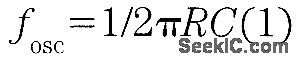


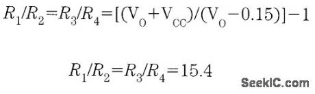


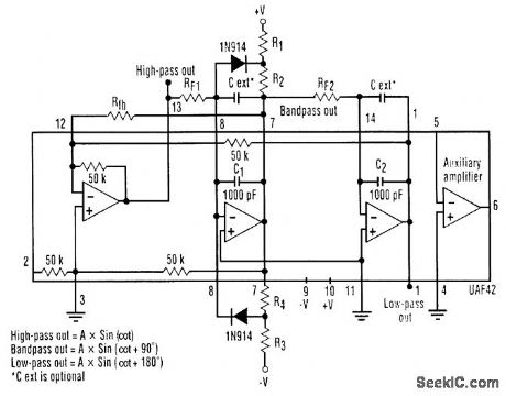


It is possible to build a three-phase sine-wave oscillator using just one UAF42 state variable filter along with some resistors and diodes. Three output nodes are available: high-pass out, bandpass out, and low-pass out. The signals at the bandpass and low-pass out nodes are 90°and 180° out of phase, respectively, with those at the high-pass out node. An on-board auxiliary op amp is available for use as a buffer or gain stage. The frequency of oscillation is set with resistors RF1 and RF2 using the simple equation:The maximumfosc obtainable using the UAF42 state-variable filter is 100 kHz. However, distortion becomes a factor for frequencies above 10 kHz. Resistance R1, R2, R3, and R4, should be selected using the following equation to set the desired signal amplitude:Resistor Rfb provides a positive feedback path from the bandpass out node to the summing-amplifier input. This provides the necessary startup required to begin oscillation. Suggested values are as follows:To design a 1-kHz,1.2-V peak oscillator,use Eq 1 to calculate RF1 and RF2∶Use Eq.2 to determine values for the signal magnitude-setting resistances R1/R2 and R3/R4:Setting R1 and R3 equal to 15.4 kΩ and R2 and R4 equal to 1 kΩ would provide the proper resistor ratios These resistors act as loads to the internal op amp (View)
View full Circuit Diagram | Comments | Reading(1129)
7_71_MHz_VFO
Published:2009/7/13 22:51:00 Author:May
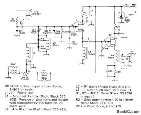
JFET Q1 serves as oscillator, with frequency determined by C2, L2, CR2, and CR3; diodes operate in reverse-bias regions as voltage-variable capacitors. Amount of reverse bias applied by R2 determines capacitance and frequency. VFO operates on both transmit and receive; on transmit, no voltage is applied to VFO offset circuit R1-C1-CR1 so it has little effect on oscillator, 0n receive, +12 V applied to R1 makes CR1 conduct and places C1 across frequency-determining network to shift VFO about 100 kHz away from operating frequency so receiver will not be blocked. Q2 is buffer between oscillator and transmitter. VR1 provides regulated 9.1 V for oscillator and buffer. (Project was named after chopped beef can in which it was mounted.)-J. Rusgrove, The CB Slider, OST, March 1977, p 15-17. (View)
View full Circuit Diagram | Comments | Reading(1321)
CUBE_GENERATOR
Published:2009/7/13 22:21:00 Author:May
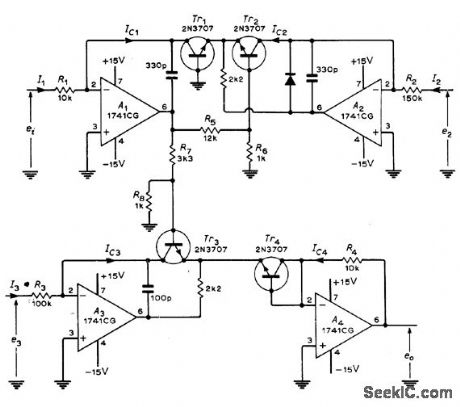
Combin ation of temperature-compensated opamp log converter and antilog converter generates output signal eo proportional to cube of input signal ei. Article gives design equations.-G. B Clayton, Experiments with Operational Amplifiers, Wireless World, Feb. 1973, p 91-93.
(View)
View full Circuit Diagram | Comments | Reading(1628)
LINEAR_SAWTOOTH_WAVEFORM_GENERATOR_CIRCUIT
Published:2009/7/13 22:20:00 Author:May
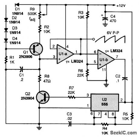
In this circuit, Q1 is a constant-current source, whose output is controlled by R9. C1 charges linearly, and follower U1-a drives comparator U1-b. When the threshold set by R3 and R6 is reached, U1-b changes state and triggers pulse generator U2, gating on Q2 and discharging C1 through R8.The cycle then repeats. The period is approximately 8 x C1/I1, where I1, is the collector current of Q1, as set by R9 and the base bias on Q1. (View)
View full Circuit Diagram | Comments | Reading(1588)
LINEAR_SAWTOOTH_GENERATOR
Published:2009/7/13 22:17:00 Author:May
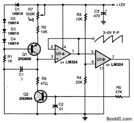


Q1is connected in a simple constant-current generator circuit. The value of Q1's emitter resistor sets the constant-current level flowing from the transistor's collector to the charging capacitor (C1).One op amp of an LM324 quad op amp IC, U1-a, is connected in a voltage-follower circuit. The input impedance of the voltage follower is very high and offers little or no load on the charging circuit. Thefollower's output is connected to the input of U1-b, which is configured as a voltage comparator. The comparator's other input is tied to a voltage divider, setting the input level to about 8 V. The output of U1-b at pin 7 switches high when the voltage at its positive input, pin 5, goes above 8 V. That turns on Q2, discharging C1. The sawtooth cycle is repeated over and over as long as power is applied to the circuit. The sawtooth's frequency is determined by the value of C1 and the charging current supplied to that capacitor. As the charging current increases, the frequency also increases, and vice versa. To increase the generator's frequency range, decrease the value of C1, and to lower the frequency, increase the value of Cr. The output is about 3 to 5 V. (View)
View full Circuit Diagram | Comments | Reading(0)
SIMPLE_SAWTOOTH_WAVEFORM_GENERATOR
Published:2009/7/13 22:12:00 Author:May
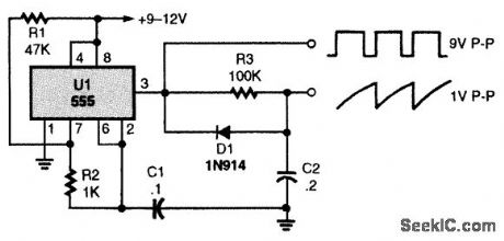
This sawtooth generator is built around a 555 configured as an astable multivibrator. (View)
View full Circuit Diagram | Comments | Reading(1182)
4224_MHz_CRYSTAL_OSCILLATOR
Published:2009/7/13 22:05:00 Author:May
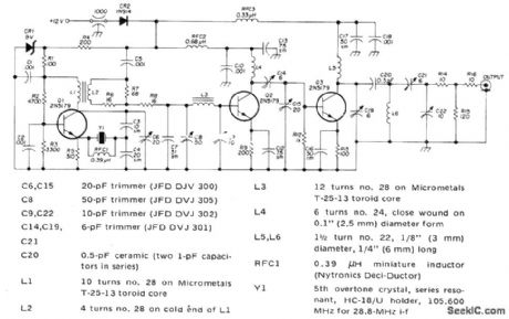
Uses 105.6-MHz crystal oscillator followed by frequency-doubling stages to give desired output for driving external diode-type tripler for which circuit is also given in article, Developed for use in 1296-MHz SSB transceiver for 23-cm amateur band.-H. P. Shuch, Easy-to-Build SSB Transceiver for 1296 MHz, Ham Radio, Sept. 1974, p 8-23. (View)
View full Circuit Diagram | Comments | Reading(1995)
6545_6845_MHz_VFO
Published:2009/7/13 22:03:00 Author:May
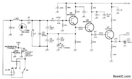
Covers 40-meter amateur band of transceiver for SSB and CW with stable incremental tuning circuit using Motorola MV1654 varactor diode CR3. Tuner permits up to 10-kHz offset above or below VFO frequency. Varactor control voltage is set by offset tuning control R3. R4 compensates for differences in varactors and adjusts VFO for zero off-set. Output buffering is provided by Q6 and Q7, with 07 also serving as power amplifier for balanced mixer used in companion exciter of transmitter. S2 activates receiver offset. Relay K1 automatically turns off offset when receiver is in transmit or standby mode, Offset feature is needed only if there is frequency difference between transmitted and received signals. L4 has 5 turns No. 22 on 1/2-inch slug-tuned ceramic form.-W. J. Weiser, Simple SSB Transmitter and Receiver for 40 Meters, Ham Radio, March 1974, p 6-20. (View)
View full Circuit Diagram | Comments | Reading(2252)
MAX038_FUNCTION_GENERATOR_
Published:2009/7/13 21:53:00 Author:May
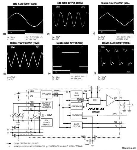

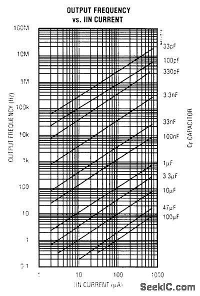
The MAX038 is a precision, high-frequency function generator that produces accurate sine, square, triangle, sawtooth, and pulse waveforms with a minimum of external components. The internal 2.5-V reference (plus an external capacitor and potentiometer) lets you vary the signal frequency from 0.1 Hz to 20 MHz. An applied ± 2.3-V control signal varies the duty cycle between 10 and 90 percent, enabling the generation of sawtooth waveforms and pulse-width modulation. A second frequency-control input-used primarily as a VCO input in phase-locked-loop applications-provides ± 70 percent of fine control. This capability also enables the generation of frequency sweeps and frequency modulation. The frequency and duty-cycle controls have minimal interaction with each other. All output amplitudes are 2 VP-P, symmetrical about ground. The low-impedance output terminal delivers as much as ± 20 mA, and a two-bit code applied to the TTL-compatible A0 and Al inputs selects the sine, square, or triangle output waveform: A0 A1 WAVEFORM X 1 sine wave 0 0 Square wave 1 0 Triangle waveX=Don’t Care (View)
View full Circuit Diagram | Comments | Reading(2421)
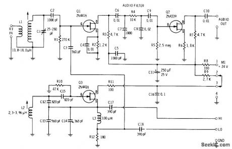
18_2_MHz_FRONT_END
Published:2009/7/16 3:15:00 Author:Jessie
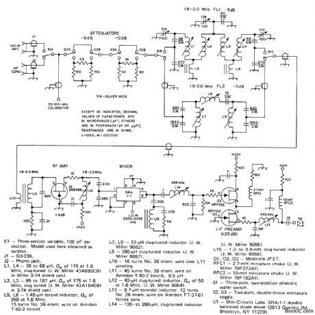
Includes enough attenuation for comfortable listening even when nearby high-power amateur station comes on air. Used with downconverter to cover 80 meters through 10 meters. Fixed-tuned 1.8-2 MHz bandpass filter FL2 eliminates need for repeaking three-pole tracking filter FL1 when tuning in band. RF amplifier Q1 compensates for filter loss by giving maximum of 6-dB gain. Double-balanced diode-ring mixer U1 handles high signal levels and has good port-to-port signal isolation. High-pass diplexer network at output of IC mixer U1 improve noise performance without degrading 455-kHz IF. Output goes to IF filter. Two-part article all other circuits of receiver. -D. DeMaw, His Eminence-the Receiver, QST, Part 1- June 1976, p27-30 (Part 2-July 1976, p 14-17).
(View)
View full Circuit Diagram | Comments | Reading(1346)
TRANSFLUXOR_OSCILLATOR
Published:2009/7/16 3:15:00 Author:Jessie
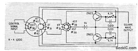
Holds frequency setting for many hours after removal of control signal. Operates between 100 kc and 1 Mc. Gives square-wave output.-R. J. Sheirn, Transfluxor Oscillator Gives Drift-Free Output, Electronics, 33:10, p 48-49. (View)
View full Circuit Diagram | Comments | Reading(1511)
MONOCHROMATOR_PREAMP
Published:2009/7/16 3:13:00 Author:Jessie
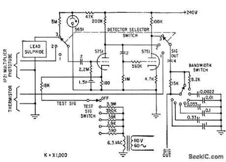
Used in scanning missile plumes to identify missile. Input may be either multiplier phototube or lead sulfide detector covering range from 0.35 micron in visible spectrum to 2.9 microns in infrared. Bias for lead sulfide detector is provided by 5651 regulator across plate supply. Test voltage is fed to cathode of first stage for gain calibration.-J. N. Day, Jr., Spectrometric Analysis of Missile Flights, Electronics, 33:21, p 86-88. (View)
View full Circuit Diagram | Comments | Reading(795)
NINE_BIT_WORD_GENERATOR
Published:2009/7/16 3:13:00 Author:Jessie
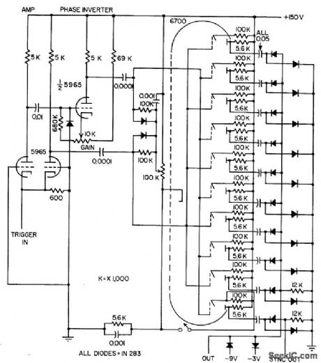
Beam-switching tube provides arbitrary nine-bit words at pulse rates from few cps to 1 Mc, for testing digital systems. Output can be changed from spike to square wave by changing plug-in capacitors.-R. R. Hartel, Word Generator for Digital Testing, Electronics, 31:9, p 71. (View)
View full Circuit Diagram | Comments | Reading(840)
2_23_MHz_UNTUNED_OSCILLATOR
Published:2009/7/13 21:37:00 Author:May
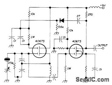
Two dualgate MOSFETs operate in untuned Colpitts crystal oscillator Used in SSB transceiver made by Sideband Associates for radiomarine communication in 2-23 MHz range Oscillator feeds isolating amplifier,Small capacitor can be used for netting individual crystal to precise assigned frequency.-E Noll, MOSFET Circuits, Ham Radio Feb 1975,p50-57. (View)
View full Circuit Diagram | Comments | Reading(1508)
PLL_AM
Published:2009/7/16 2:28:00 Author:Jessie
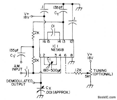
Phase-locked loop of Signetics NE561B is locked to AM signal carrier frequency, and output of VCO in IC is used as local oscillator signal for product detector. Tuned RF stage will generally be required, along with good antenna and ground. Simple one-transistor audio amplifier will suffice for driving loud-speaker. Circuit can be adapted for other frequencies outside of broadcast band, from 1 Hz to 15 MHz, by changing values of CY and C1.-E.Kanter, PLL IC Applications for Hams, 73 Magazine, Sept. 1973, p 47-49. (View)
View full Circuit Diagram | Comments | Reading(1976)
| Pages:67/195 At 206162636465666768697071727374757677787980Under 20 |
Circuit Categories
power supply circuit
Amplifier Circuit
Basic Circuit
LED and Light Circuit
Sensor Circuit
Signal Processing
Electrical Equipment Circuit
Control Circuit
Remote Control Circuit
A/D-D/A Converter Circuit
Audio Circuit
Measuring and Test Circuit
Communication Circuit
Computer-Related Circuit
555 Circuit
Automotive Circuit
Repairing Circuit