
Signal Processing
Index 76
LINEAR_VCO
Published:2009/7/11 4:02:00 Author:May
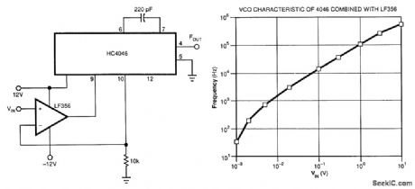
This VCO uses an LF356 op amp to produce a linear frequency vs. voltage characteristic using the CMOS HC4046. The frequency range can be changed by changing the capacitor connected between pins 6 and 7 of the HC4046. Using the HC4046's internal transistor instead of an external component achieves the linearization in Fig. 98-5(b). (View)
View full Circuit Diagram | Comments | Reading(3364)
SIMPLE_555_VCO
Published:2009/7/11 3:59:00 Author:May
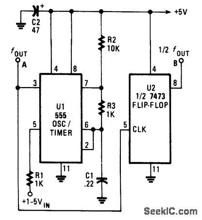
The VCO has an output frequency that ranges from 1 500 Hz at Vin=1 V to 300 Hz at Vin=5V. R1 or C1 can be varied to change this range. U2 provides a symmetrical square-wave output of half the timer frequency. (View)
View full Circuit Diagram | Comments | Reading(1406)
__RESTRICTED_RANGE_VCO
Published:2009/7/11 3:57:00 Author:May

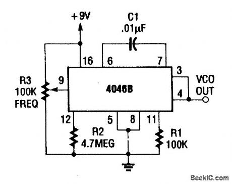
This VCO is adjustable from 60 Hz to 1.4 kHz. C1 can be changed for other ranges (View)
View full Circuit Diagram | Comments | Reading(1308)
REGENERATIVE_SHORTWAVE_RECEIVER
Published:2009/7/17 2:46:00 Author:Jessie
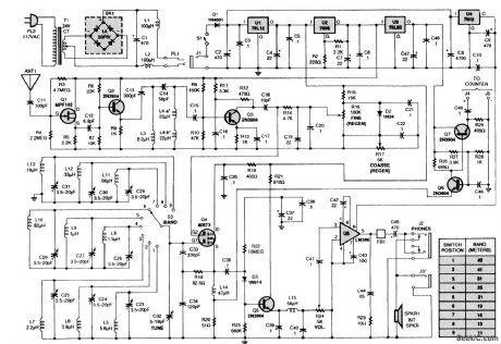
The receiver is composed of several subassemblies: an active antenna, an amplifier (with a regeneration control and band-switching circuitry), an AM detector, a power amplifier, and some form of output device (internal speaker, external speaker, or phones), plus a multivoltage power supply. The schematic diagram of the receiver is shown in the figure, a dual-gate MOSFET, Q4 (which is analogous to a pentode vacuum tube), is used as the regenerative amplifier. The dual-gate MOSFET is configured as a Colpitts oscillator, rather than an Armstrong type. The MOSFET's feedback from source to gate is provided via R18 and C33. The circuit contains several standard fixed-value inductors, each of which is connected in parallel with a small variable capacitor. Those LO pairs along with a SP12T rotary switch (S2) are used for band selection. Regenerative amplification and AM detection are performed by two separate transistors, Q4 and Q5. The AM detector (which is called an infinite-irnpedance detector) has the advantage of not loading the RF stage appreciably, Because D3 is operated with a slight forward bias, either a germanium or a silicon diode can be used in that position. The dc voltage across R24 (the volume control) should be about 0.1 V. Regeneration is controlled by varying the voltage applied to gate 2 of Q4. The circuit also contains fine and coarse regeneration controls that allow delicate adjustments. The receiver uses an active-antenna circuit, consisting of transistors Q1, Q2, and Q3. Under most conditions, a short whip antenna is adequate. (View)
View full Circuit Diagram | Comments | Reading(5190)
__GATED_WIDE_RANGE_VCO
Published:2009/7/11 3:49:00 Author:May
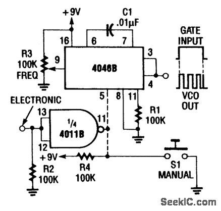
A CD4046 can be gated either with a switch or electronically, as shown in the figure. Frequency range of this circuit is to 1.5 kHz; use another C1 for higher frequencies. (View)
View full Circuit Diagram | Comments | Reading(1323)
SIMPLE_AUDIO_FREQUENCY_VCO
Published:2009/7/11 3:47:00 Author:May
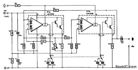
The frequency of this sine-wave oscillator is determined by a direct voltage, UC, of 0 to 15 V. The distortion on output signals of up to 10 Vpp is not greater than 1%. When the output is reduced with the aid of Pl to 1 Vpp, the distortion drops to below 0.1% It is not recommended to use output signals below 1 Vpp, because the oscillator then becomes unstable and temperature-dependent.The oscillator consists of two operational transconductance amplifiers (OTAs) contained in one package. Their Amp-bias inputs, pins 1 and 16, are connected in parallel. These inputs can drive the output currents at pins 5 and 12 to a peak value of up to 0.75 mA.Switch S1 enables the oscillator output to be set to two ranges: 6.7 to 400 Hz and 400 Hz to 23.8 kHz.The overall range needs a control voltage that varies from 1.34 to 15 V. When the frequency is changed by a variation of UC and the setting of P1 is not altered, the output signal might be distorted. In other words, the amplitude of the signal must be adapted to the frequency. (View)
View full Circuit Diagram | Comments | Reading(2233)
VLF_HF_LIGHTNING_DETECTOR_RECEIVER
Published:2009/7/17 2:40:00 Author:Jessie
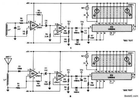
It is known that cloud-to-ground lightning strikes produce far more VLF emissions than cloud-to-cloud strikes. By monitoring both VLF and HE, lightning can be analyzed for such things as strikes per flash, leader steps, amplitude or relative range, and the ratio of cloud-to-ground to cloud-to-cloud discharge. This pair of simple receivers separately monitor both VLF and HE. Note that they are both extremely similar, except for their respective antenna coils. The VLF-antenna coil, L1 in Fig. A, is made of 94 turns of #33 magnet wire wound on an 11-inch-diameter cardboard disk. The HE-antenna coil, L1 in Fig. B, is a common RF choke, or about 100 turns of very fine magnet wire on a X-inch-long ferrite core (any similar junkbox choke should do). Antenna ANTI is a 6-inch wire an-tenna. The first LF411 FET op amps (IC1 in both circuits) are preamps. The second LF411s (IC2 in both) add more gain. Test point 1 in either circuit can be used to connect high-impedance head-phones or an oscilloscope. Test point 2 in either circuit is for a connection to chart recorders or event counters. The outputs of both circuits go to LM3914 bar-graph display drivers (IC3 in both circuits), which power both LED bar graphs (DISP1 in both) and low-voltage piezo buzzers (BZ1, again in both receivers). The negative leads of the buzzers, while shown connected to pin 1, can be connected to any of the bar-graph outputs. Both circuits are powered by split supplies. (View)
View full Circuit Diagram | Comments | Reading(10300)
KEYER_OSCILLATOR
Published:2009/7/11 3:24:00 Author:May
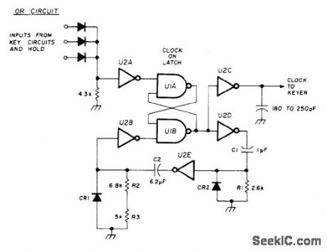
Oscillator or clock starts when key is closed and can be held until dot, dash, or space is completed. U1 is SN7400, and U2 is SN74L04. Diodes at input of U2A form OR gate that controls oscillator. These inputs can be used to keep oscillator running for self-completing action. Time constant, set by C1 and R1, is 4 ms which is width of clock pulse. Values for C2, R2, and R3 give pulse repetition rate of 50 to 95 ms, comesponding to about 12 to 24 WPM.For higher speeds, reduce values of C2 and R2.CR1 and CR2 are signal diodes that prevent first pulse from being different; 250-pF capacitor on output prevents noise spikes from triggering keyer circuits falsely.-J. T. Miller, Integrated-Circuit Oscillator, Ham Radio, Feb. 1978, p 77. (View)
View full Circuit Diagram | Comments | Reading(1508)
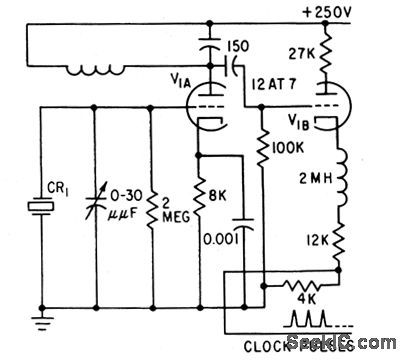
SIDEREAL_REGENERATIVE_OSClLLATOR
Published:2009/7/11 3:19:00 Author:May
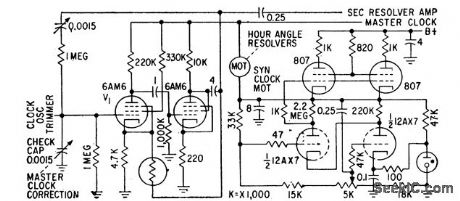
Compares synchronous clock motor speed at 30-sec intervals with pendulum-driven master sidereal-time clock. Motor runs slightly faster than sidereal lime. If too fast at checking time, check capacitor at input of V1 is closed to reduce frequency of oscillation ond speed of motor to bring it back into coinddence with master.-C.N. Kingston, Radio Telescope Sees 2 Billion Light Years, Electronics, 31:23, p70-75. (View)
View full Circuit Diagram | Comments | Reading(807)
PSEUDORANDOM_DIGITAL_GENERATOR
Published:2009/7/11 3:19:00 Author:May
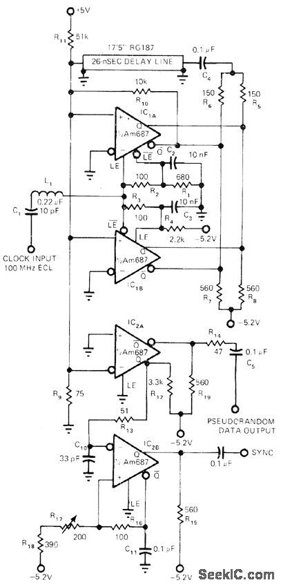
Uses two Am687 dual sampling comparators toimplement 200-Mb/s pseudorandom digital-sequence generator for checking and measuring performance of high-speed digital communication equipment. Produces sequence length of 127 bits, but delay-line length can be changed to give any desired other sequence length. Circuit acceptsfrom 195to 203 Mb/s,which is more than adequate for systems using crystal clock having ±0.1% frequency variation. Article describes operation and gives timing diagram.-G. L. Meyer, Sampling Comparators-They Sub for High-Speed Logic and Produce Power, Cost and Space Savings, EDN Magazine, Sept. 5,1977, p 71-74. (View)
View full Circuit Diagram | Comments | Reading(834)
10_MC_CLOCK_OSCILLATOR
Published:2009/7/11 3:02:00 Author:May

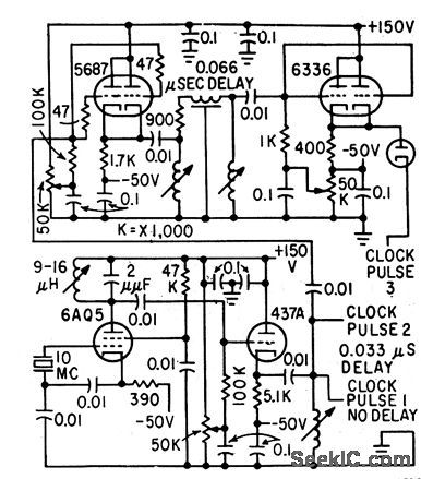
Output through cathode follower is split into three channels(two are not shown) to get clock pulses at three phases.-G,O. Olson,Design of High-Frequency clock Pulse Generators Electronics,32:35,p56-57. (View)
View full Circuit Diagram | Comments | Reading(691)
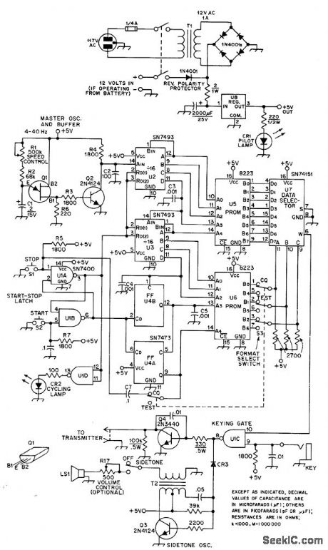
CW_CALL_GENERATOR
Published:2009/7/11 2:58:00 Author:May
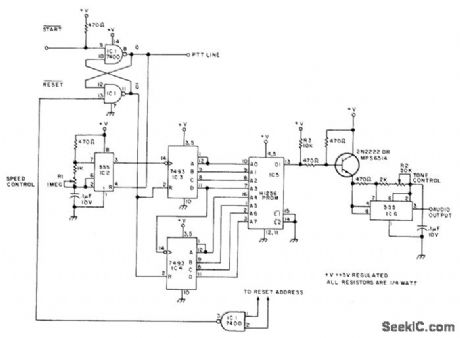
Basic CW identifier uses two gates of 7400 to form starting flip-flop of automatic message generator. Provides ad-iustable speed and tone, with up to 256 bits of storage in Harris H1256 PROM. IC2 is 555 astable MVBR providing clock signal for driving two 7493 4-bit binary counters that address PROM.When counters reach maximum address of 255, next clock count makes PROM restart at address 0. Each address turns on tone oscillator for one clock period, producing one dit. Three addresses in row turn on tone for three clock periods, producing one dah. Space between dits and dahs of same letter is equal to one dit, letter space is three dits, and word space is six dits (2 dahs). Thus,W takes nine addresses. Article describes operation in detail and tells how to modify circuit for use as RTTY message gen-erator.-R. B. Joerger, PROM Message Generatorfor RTTY, 73 Magazine, March 1977, p 94-98. (View)
View full Circuit Diagram | Comments | Reading(1486)
COLOR_BAR_GENERATOR
Published:2009/7/11 2:51:00 Author:May
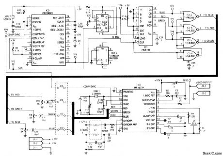
IC5 generates RS-170 NTSC synch.IC1,IC2 and IC3 make up the red,green,and blue video signals that drive the videoencoder section of IC6 to make up the color bars. IC3 is an a÷2 counter that drives 4-bit counter IC1.Gates IC2a through IC2b formthe R,B,and G,Video signals.IC6 encodes these,plus synch,to form an NTSC video output signal,which appears at TP12. (View)
View full Circuit Diagram | Comments | Reading(4146)
809_11_KC_CLOCK_OSCILLATOR
Published:2009/7/11 2:41:00 Author:May
Crystctl-controlled oscillator V1A and shaping circuit V1B produce pulses with repetition rate equal to frequency of crystal oscillator.-H. Vantine Jr.and E. C. Johnson, Modified Transceivers Compute Distance, Electronics, 31:37, p94-98. (View)
View full Circuit Diagram | Comments | Reading(822)
REGENERATED_CW
Published:2009/7/11 2:41:00 Author:May
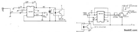
Audio oscillator whose frequency can be varied is keyed in accordance with incoming CW signal, to give clean locally generated audio signal without background noise and interference. NE567 phase-locked loop serves as tunable audio filter and LED switch driver for activating NE555 variable-frequency tone oscillator. LED serves as visual tuning aid to indicato that PLL is looked on to incoming signal.-Regenerated CW.73 Magazine, Dec. 1977,p152-153. (View)
View full Circuit Diagram | Comments | Reading(1696)
CLOCK_PULSE_GENERATOR
Published:2009/7/11 2:37:00 Author:May
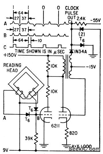
Derives pulse from reading head that scans data track of magnetic-spoke disk memory, eliminating need for separate timing track. Generates pulse for each magnetic spoke passing over gap of head, regardless of whether spoke is written with 1 or 0.-T. C. Chen and O. B. Stram, Digital Memory System Keeps Circuits Simple, Electronics, 32:11, p130-133. (View)
View full Circuit Diagram | Comments | Reading(864)
AF_OSCILLATOR_MONITORS_CW
Published:2009/7/11 2:29:00 Author:May
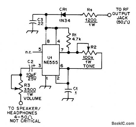
Can be added to any transceiver not already having built-in sidetone oscillator, to hear keying of transmitter. RF input from transmitter is rectified by CR1 to provideabout 6-VDC supply. Keying of carrier on and off tums NE555 AF oscillator on and off correspondingly.-J. Amold, A CW Monitorfor the Swan 270, QST, Aug. 1976, p 44. (View)
View full Circuit Diagram | Comments | Reading(1185)
SIMPLE_TRF_RECEIVER
Published:2009/7/17 3:29:00 Author:Jessie
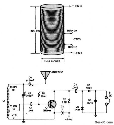
Here is a receiver that contains an RF amplifier. The desired radio-frequency signal can be selected by tuning C5. (View)
View full Circuit Diagram | Comments | Reading(2499)
CLOCK_OSCILLATOR
Published:2009/7/11 2:18:00 Author:May
Q11 and Q2 form oscillator section of tim-base generator, and Q3-Q4 serve as pulse shaper. Q1 is grounded-base voltage amplifier with tuned collector load.Q2 matches impedance of Q1 collector circuit to crystal. Output amplitude is limited by zener diode D1-R.S. Reed,Rugged Arming-Fuzing Timer for Atomic Artillery Mssile Electronics,34:38,p48-51. (View)
View full Circuit Diagram | Comments | Reading(1005)
SOLID_STATE_REGENERATIVE_RECEIVER
Published:2009/7/17 3:26:00 Author:Jessie
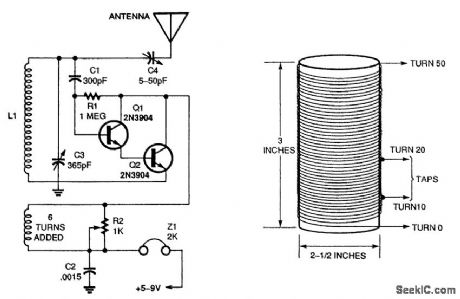
You will need to modify the coil shown to use it with the regenerative receiver. Place a single layer of electrical tape around the bottom winding of the coil (L1); wind 6 turns of 19- or 20-gauge wire over the taped winding, leaving 4 pigtails. Tape the winding in place. Then connect the modified coil to the receiver circuit as shown in the figure. The two 2N3904 transistors are connected in a Darlington high-input-impedance circuit configuration to reduce loading of the tuned circuit. Potentiometer R2 controls the positive RE feedback. If the receiver seems dead or if only weak signals are heard, try reversing the leads on the six-turn feedback coil. (View)
View full Circuit Diagram | Comments | Reading(4792)
| Pages:76/195 At 206162636465666768697071727374757677787980Under 20 |
Circuit Categories
power supply circuit
Amplifier Circuit
Basic Circuit
LED and Light Circuit
Sensor Circuit
Signal Processing
Electrical Equipment Circuit
Control Circuit
Remote Control Circuit
A/D-D/A Converter Circuit
Audio Circuit
Measuring and Test Circuit
Communication Circuit
Computer-Related Circuit
555 Circuit
Automotive Circuit
Repairing Circuit