
Signal Processing
Index 68
6_METER_FRONT_END
Published:2009/7/16 2:27:00 Author:Jessie
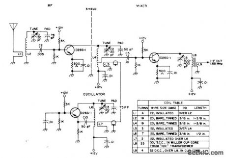
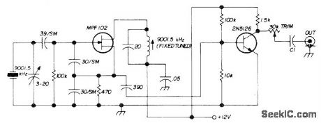
Developed for use as converter with any communication receiver having 1.65-MHz IF. Article covers construction and tune-up. Use of GE microtransistors permits miniaturization.-B. Hoisington, A Real Hot Front End for Six, 73 Magazine, Nov. 1974, p 88-90 and 92-94. (View)
View full Circuit Diagram | Comments | Reading(1093)
BALANCED_MIXER
Published:2009/7/16 2:26:00 Author:Jessie
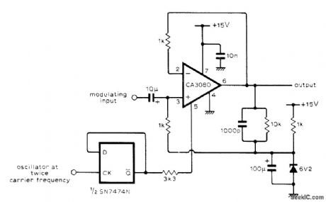
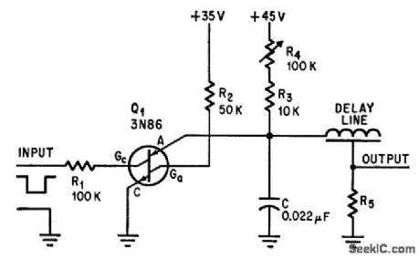
Uses CA3080 IC transconductance amplifier as precise low-frequency single balanced mixer with inherent carrier balance and accurately defined conversion gain. Binary divider IC halves oscillator frequency, giving carrier waveform having highly accurate unity mark-space ratio. Divided carrier is used to switch amplifier on as unity-gain voltage follower. Conversion loss is 4 dB.-R. J. Harris, Single Balanced Mixer, Wireless World, May 1976, p 79. (View)
View full Circuit Diagram | Comments | Reading(2268)
SYNCHRONOUS_AM_DETECTOR
Published:2009/7/16 2:24:00 Author:Jessie
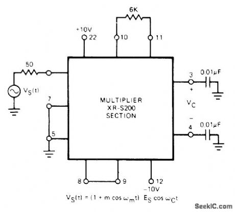
Input signal is applied to multiplier section of Exar XR-S200 PLL IC with pins 5 and 7 grounded. Detector gain and demodulated output linearity are then determined by resistor connected between pins 10 and 11, in range of 1K to 10K for carrier amplitudes of 100 mV P-P or greater. Multiplier output can be low-pass filtered to obtain demodulated output, For typical 30% modulated input with 10-MHz carrier and 1-kHz modulation, output is clean 1-kHz sine wave.- Phase-Locked Loop Data Book, Exar Integrated Systems, Sunnyvale, CA, 1978, p 9-16. (View)
View full Circuit Diagram | Comments | Reading(1080)
ADJUSTABLE_RISE_AND_FALL_TIMES
Published:2009/7/16 2:23:00 Author:Jessie
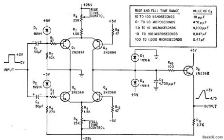
constant-current source Q1-Q2 charges C3,while Constany-current sink Q3-Q4 discharges C3.-D. N Lee, Rise Time Adjustment Independent Of Fall Time, Electronics, 38:2 p76-78.
(View)
View full Circuit Diagram | Comments | Reading(1162)
SINGLE_SCS
Published:2009/7/16 2:22:00 Author:Jessie
R4 varies relaxation frequency of pnpn silicon controlled switch from 1 to 500 pps, independently of pulse duration and amplitude. For operation in gated mode, cathode gate pulse at input should be -1.5. v at 50 microamp.-H. H. Wieder, Silicon Controlled Switch Con Generate Pulses, Electronics, 38:2, p 79. (View)
View full Circuit Diagram | Comments | Reading(772)
9_MHz_CRYSTAL
Published:2009/7/13 21:27:00 Author:May
Used in transmitter section of 80-meter 10-W SSB transceiver. Value of C1 is 50-330 pF, chosen for desired output range. Carrier level can be adjusted with slug-tuned coil or with 30K trimpot.-D. Hembling, Solid State 80-Meter SSB Transceiver, Ham Radio, March 1973, p 6-17. (View)
View full Circuit Diagram | Comments | Reading(1627)
AM_SUBSYSTEM
Published:2009/7/16 2:13:00 Author:Jessie
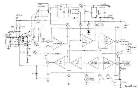
Single RCA CA3088E IC serves as AM converter, IF amplifier, detector, and preamp for AM broadcast or communication receiver. RF amplifier stage using RCA 40841 dual gate-protected MOSFET is optional. IC also provides internal AGC for first IF stage and delayed AGC for optional RF stage. Internal buffer stage can be used to drive tuning meter.- Linear Integrated Circuits and MOS/ FET's , RCA Solid State Division, Somerville, NJ, 1977, p 348-349. (View)
View full Circuit Diagram | Comments | Reading(1306)
SIMPLE_PLL_DEMODULATOR
Published:2009/7/16 2:11:00 Author:Jessie
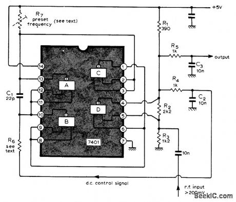
Requires only single IC to provide synchronous detection. Performance is satisfactory for most requirements of most amateur radio experimenters. Gates A, B, and C in IC form relaxation-type VCO whose output frequency is determined by C1 and positive current sources supplying pins 10 and 13 of IC. When pin 6 is high, gate D is biased by R2 and R3 to operate as linear amplifier for input signal. In operation, pin 6 is made alternately high and low by oscillator output, so D acts as amplifying phase detector. Output goes through low-pass filter R4-C2 to VCO, completing phase-locked loop. Separate filter R5-C3 provides AF output. When C1 is 22 pF, circuit operates at about 10 MHz. With 270 ohms for R6, lock is maintained over range of 2 MHz; with 10 kilohms, locking range is 300 kHz. R7 is optional, for fine adjustment of frequency.-R. King, Phase-Locked Loop Demodulator, Wireless World, July 1973, p 337. (View)
View full Circuit Diagram | Comments | Reading(928)
UNIJUNCTION_TRANSISTOR_GENERATES_DESIRED_NUMBER_OF_PULSES
Published:2009/7/16 2:04:00 Author:Jessie
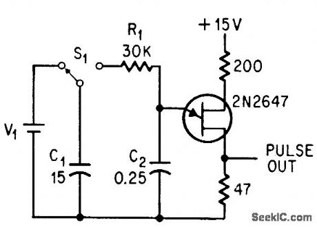
Number of pulses generated each time switch St is operated increases linearly from 0 to 140 as battery voltage is increased from 11 to 35 v. Charge transferred from C1 to C2 fires transistor , discharging C2, with cycle repeating until C2 voltage drops below firing point.-R. Ferrie, Unijunction Circuit Generates Specific Number of Pulses, Electronics, 37:15, p 78. (View)
View full Circuit Diagram | Comments | Reading(847)
SYNCHRONIZED_MAX038_FUNCTION_GENERATORS
Published:2009/7/13 21:24:00 Author:May

The MAX038's internal phase detector is intended primarily for use in phase-locked-loop (PLL) configurations. In (a), for example, the phase detector in IC2 enables that device to synchronize its operation with that of IC1. You connect the applied reference signal to IC2's TTL/CMOS-compatible phase-detector input (PDI) and connect the phase-detector output (PDO) to the input (FADJ) of the internal voltage-controlled oscillator. PDO is the output of an exclusive-OR gate-a mixer-which produces rectangular current waveforms at frequencies equal to the sum and difference of the PDI frequency and the MAX038 output frequency. These waveforms are integrated by CPD, to form a triangle-wave voltage output at PDO (b). The 10-Ω/100-pF pair at PDI limits that pin's rate of rise to 10 ns. (View)
View full Circuit Diagram | Comments | Reading(2413)
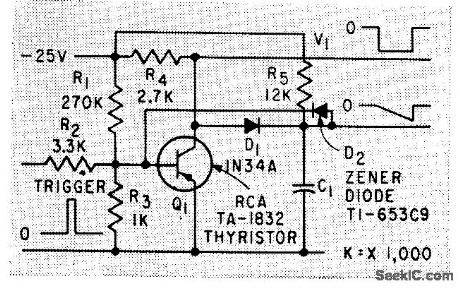
TUNNEL_DIODE_PULSER
Published:2009/7/16 2:03:00 Author:Jessie
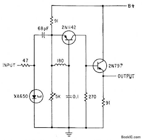
Switching voltage change of tunnel diode is differentiated and amplifed by grounded-base amplifer. With 8-V supply, 5-V output pulses are obtained into 91 ohms at clock rates up to 140 Mc.-M. V. Harrison and R. S. Foote, Tunnel Diodes Increase Digital-Circuit Switching Speeds, Electronics, 34:32 p154-156. (View)
View full Circuit Diagram | Comments | Reading(1235)
160_500_MHz_DIODE_RECEIVER
Published:2009/7/16 1:55:00 Author:Jessie
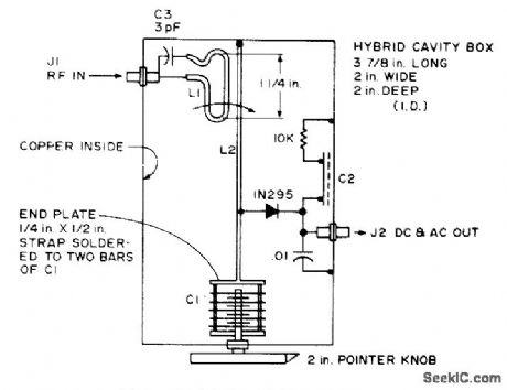
Cavity version of basic crystal detector was developed for use chiefly in 220-MHz and 450-MHz amateur bands. C1 is 25-pF tuning capacitor, and C2 is 1 x 2 inch brass plate insulated from sheet-copper cavity by 0.005-inch Teflon sheet or mica. L1 is 3-inch length of 1-inch copper strap.-B. Hoisington, Tuned Diode VHF Receivers, 73 Magazine, Dec. 1974, p 81-84. (View)
View full Circuit Diagram | Comments | Reading(1050)
ULTRASONIC_RECEIVER
Published:2009/7/16 1:54:00 Author:Jessie
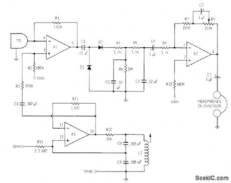
Amplifies output of 40-kHz ultrasonic transducer M1 by mixing in opamp A1 with signal of local oscillator A3 to produce AF signal for further amplification by A2 which drives headphones. Opamp sections are from Motorola MC3401P quad opamp. Diodes are 1N914 or equivalent, L1 is Miller 6315 4-30 mH Supply can be 9-12V,Transmitter can be wide-range audio amplifier capable of handling 38-42 kHz, driving similar ultrasonic transducer. -C. D. Rakes, Integrated Circuit Projects, ″ Howard W. Sams, Indianapolis, IN, 1975, p 26-29. (View)
View full Circuit Diagram | Comments | Reading(6298)
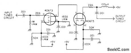
2945_MHz_PREAMP
Published:2009/7/16 1:52:00 Author:Jessie
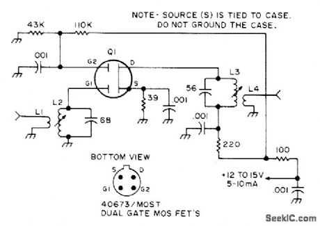
Reduces noise figure of average communication receiver 2.5 dB and adds up to 20 dB of gain, as required for reception of 29.45-MHz satellite beacon signals. Q1 is RCA 40673 or almost any other dual-gate MOS-FET, with shield partition across the device. L2 is 10 turns No. 24E spaced on 1/4-inch slug-tuned core, with 2 turns over cold end for L1. L3 is 10 turns No. 24E closewound on 1/4-inch slug-tuned core, with 2 turns over cold end for L4.-J. D. Colson, An Oscar Preamp That Works Wonders, 73 Magazine, July 1975, p 31-32. (View)
View full Circuit Diagram | Comments | Reading(2948)
455_kHz_BFO
Published:2009/7/16 1:51:00 Author:Jessie
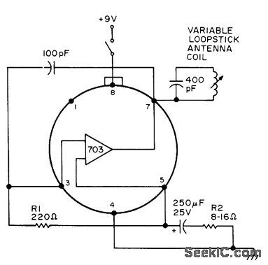
Simple basic oscillator produces signal that can be mixed with signals in all-band radio to give beat frequency for CW or SSB reception. By itself, circuit can be used as low-power (QRP) phone or CW transmitter or as signal source for other purposes.-R. L. Price, 99¢ IC BFO, 73 Magazine, Jan. 1976, p 201. (View)
View full Circuit Diagram | Comments | Reading(3262)
SIMPLE_SQUARE_WAVE_GENERATOR
Published:2009/7/16 3:19:00 Author:Jessie
Circuit performance is mode independent of active elements by using transistor only as switch. For reliable operation, circuit requires extra 10% of output-pulse-width dead time between triggers.-C. A.. Von Urff and R. W. Ahrons, How to Generate Accurate Sawtooth and Pulse Waves, Electronics, 32:50, p 64-66. (View)
View full Circuit Diagram | Comments | Reading(1349)
COMMON_BASE_BLOCKING_OSCILLATOR
Published:2009/7/16 3:16:00 Author:Jessie
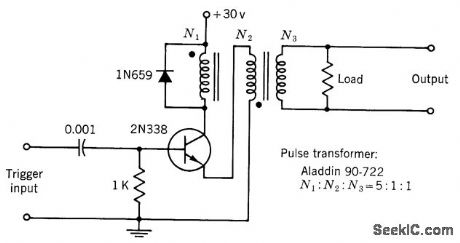
Nonsaturating-type triggered blocking oscillator is used when fast response is desired. Often used as pulse generator when waveform requirements are not critical.-Texas Instruments Inc., Transistor Circuit Design, McGraw-Hill, N.Y., 1963, p 430. (View)
View full Circuit Diagram | Comments | Reading(1181)
PREAMP_BOOSTS_GAIN_20_dB
Published:2009/7/16 3:12:00 Author:Jessie
Two RCA MOSFETs in cascode provide extra 20 dB of gain when used ahead of older Radio Shack AX-190 shortwave receiver. Input and output tuned circuits, gang-tuned, are part of receiver preselector. Article covers construction and tune-up.-P. J. Dujmich, Improve the AX-190 Receiver, 73 Magazine, Jan. 1978, p 106-107. (View)
View full Circuit Diagram | Comments | Reading(1172)
30_NSEC_5000_V_30_AMP_PULSES
Published:2009/7/16 2:57:00 Author:Jessie
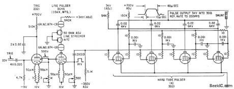
Used for testing magnetic materials at narrow pulse widths. Four hard tubes in parallel drive test cores with 0.1 megawatt peak power and give some degree of regulation during pulsing.-G. A. Reeser, How Magnetic Materials Behave at Nanosecond Pulse Widths, Electronics, 34:36, p 72-75. (View)
View full Circuit Diagram | Comments | Reading(707)
CONTROL_FOR_FISH_SHOCKER
Published:2009/7/16 2:55:00 Author:Jessie
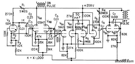
Produces liming pulses that can be varied in range of 2 to 30 cps, with durations up to 250 millisec for square waves. R1 changes frequency of oscillator V3, while C6, R4, and R5 in delay mvbr V5.V6 determine Width of pulse.-H. P. Dale, Electronic Fishing with Underwater Pulses, Electronics, 32:4, p 31-33. (View)
View full Circuit Diagram | Comments | Reading(2001)
| Pages:68/195 At 206162636465666768697071727374757677787980Under 20 |
Circuit Categories
power supply circuit
Amplifier Circuit
Basic Circuit
LED and Light Circuit
Sensor Circuit
Signal Processing
Electrical Equipment Circuit
Control Circuit
Remote Control Circuit
A/D-D/A Converter Circuit
Audio Circuit
Measuring and Test Circuit
Communication Circuit
Computer-Related Circuit
555 Circuit
Automotive Circuit
Repairing Circuit