
Signal Processing
Index 86
VERY_LOW_DISTORTION_OSCILLATOR
Published:2009/7/10 1:24:00 Author:May
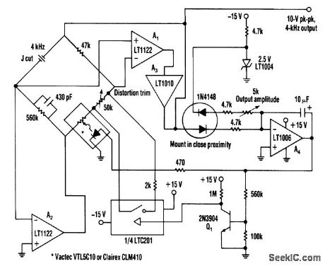
his oscillator uses a bridge circuit with an optoisolator as a gain-control device. The resultant distor-tion can be held to 9 ppm (.0009%) with proper adjustment. (View)
View full Circuit Diagram | Comments | Reading(834)
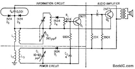
SIX_TRANSISITOR_9_V_BROASCAST_WITH_TUNED_R_F_STAGE
Published:2009/7/19 23:46:00 Author:Jessie
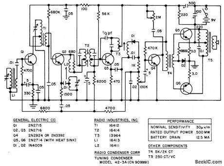
Nominal sensitivity is 30 microvolts per meter, power output 500 mw, and battery drain 12.5 ma.-“Transistor Manual,” Seventh Edition, General Electric Co., 1964, p 296. (View)
View full Circuit Diagram | Comments | Reading(734)
HIGH_STABILITY_3_35_MC_OSCILLATOR
Published:2009/7/19 23:43:00 Author:Jessie
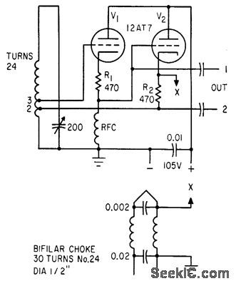
Modification of Lampkin circuit uses pair of cathode followers in cascade, with tube circuits being tapped across part of coil and excited from resonator through high impedance. Bifilar choke minimizes variations in heater-cathode capacitance of driver V2.-E. Robberson, R-F Oscillator has Improved Stability, Electronics, 36:32, p 62-63. (View)
View full Circuit Diagram | Comments | Reading(1181)
WIEN_BRIDGE_BASED_OSCILLATOR_WITH_VERY_LOW_DISTORTION
Published:2009/7/10 1:20:00 Author:May
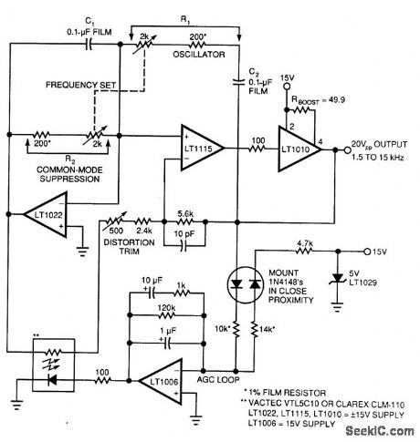
This complex oscillator circuit uses a photocell and common-mode-suppression circuitry to achieve distortion of 0.0003%. This oscillator circuit replaces the lamp in the traditional Wien bridge with an elec-tronic equivalent. (View)
View full Circuit Diagram | Comments | Reading(1054)
I_F_A_F_REFLEX
Published:2009/7/19 23:41:00 Author:Jessie
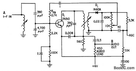
Single transistor gives simultaneous amplification at intermediate and audio frequencies in economy radio. Careful design provides high gain and sufficient un distorted output power to drive audio output transistor at full rating without motorboating.-J. Waring, How To Design Reflexed Transistor Receivers, Electronics, 32:19, p 70-72. (View)
View full Circuit Diagram | Comments | Reading(837)
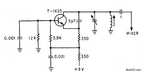
500_MC_COLPITTS
Published:2009/7/19 23:41:00 Author:Jessie
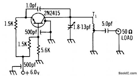
Frequency varies less than 3 Mc from 25 to 75℃, and less than 1.5 Mc with bias change from 6 to 9 V. Output is 10 mw. T1 is 1.5 length of 3/8 brass rod with output tap 1/4 from bottom.-Texas Instruments Inc., Solid-State Communications, McGraw-Hill, N.Y., 1966, p 301. (View)
View full Circuit Diagram | Comments | Reading(782)
VLF_AUDIO_TONE_GENERATOR
Published:2009/7/10 1:10:00 Author:May
Using an LC-tuned circuit, this oscillator can produce frequencies of less than 10Hz. C1 and C2 can be as large as 100μF. (View)
View full Circuit Diagram | Comments | Reading(650)
TEMPERATURE_STABLE_200_MC
Published:2009/7/19 23:40:00 Author:Jessie
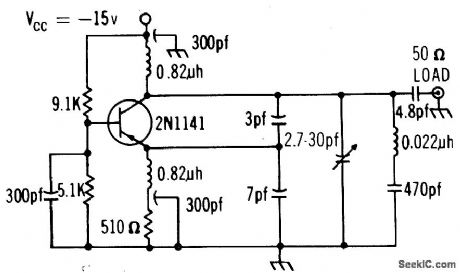
Varies less than 2 Mc in frequency and less than 1.5 mw in power output over temperature range of 25 to 80℃. Normal power output is 22.5 mw. -Texas Instruments Inc., Solid-State Communications, McGraw-Hill, N.Y., 1966, p 301. (View)
View full Circuit Diagram | Comments | Reading(798)
TWO_TRANSISTOR_SINE_WAVE_OSCILLATOR
Published:2009/7/10 1:07:00 Author:May
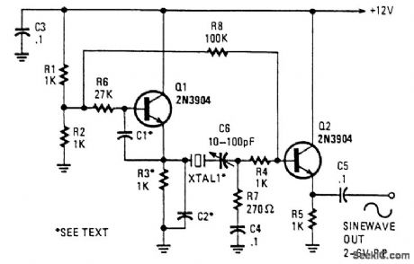
This oscillator uses two transistors and operates the crystal in the fundamental mode. C1 and C2 should be about 2 700 pF for 1 MHz, 680 pF for 5 MHz, and 330 pF for 10 MHz. 150 pF can be used for up to 20 MHz. The output is a near perfect sine wave. Try varying C1 and C2 for best waveform. About 2 to 6 Vpp is available. (View)
View full Circuit Diagram | Comments | Reading(2738)
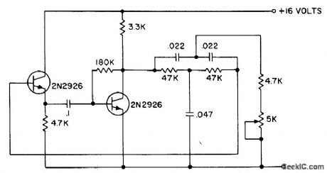
NONLINEAR_VOLTAGE_CONTROLLED_OSCILLATOR
Published:2009/7/19 23:39:00 Author:Jessie
Use of conventional transistors rather than fet's means that Q1 and Q2 operate in knee region, where frequency does not vary linearly with d-c control voltage. This is generally not a drawback when control voltage is servoed. Increasing the control voltage increases the frequency.-R. Selleck, Voltage-Controlled Oscillators, EEE, 13:3, p 47. (View)
View full Circuit Diagram | Comments | Reading(808)
60_Hz_SINE_WAVE_GENERATOR
Published:2009/7/10 1:06:00 Author:May
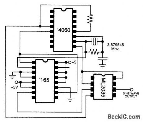
A chip by Micro Linear and two CMOS (40165 and 4060) chips generate sine waves at 60 Hz. (View)
View full Circuit Diagram | Comments | Reading(1807)
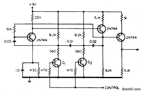
FOUR_TRANSISTOR_A_C_LINE_SET
Published:2009/7/19 23:39:00 Author:Jessie
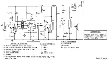
Nominal sensitivity is 40 microvolts per meter, power output 750 mw, and total power drain 10 w. - Transistor Manual, Seventh Edition, General Electric Co., 1964, p 297. (View)
View full Circuit Diagram | Comments | Reading(699)
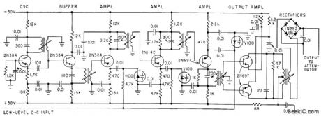
PURE_SINE_WAVE_GENERATOR
Published:2009/7/10 1:04:00 Author:May

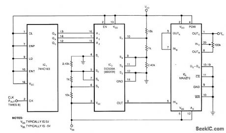
This circuit produces a pure, -80-dB THD sine wave with a frequency that is equal to thefc of IC3's filter. A TTL counter, an 8-channel analog multiplexer, and a fourth-order low-pass filter can generate 1- to 25-kHz sine waves with a THD of better than -80 dB. The circuit cascades the two second-order, contin-uous-time Sallen-Key filters within IC3 to implement the fourth-order low-pass filter. Two resistive dividers connected from ground to VDD and ground toVSS provide bipolar dc inputs to the multiplexer.To operate the circuit, you first must choose the filter's cutoff frequency, fc, by tying IC3's Do through D6 inputs to 5 V or ground. The cutoff frequency can be at 128 possible levels between 1 and 25 kHz, depending on those 7 digital input levels. Because this figure ties Do through D6 to ground, fc equals 1 kHz. The 100-kHz potentiometer adjusts the output level anywhere from 1.5 V below VDD to 1.5 V above VSS.The clock input frequency must be 8 times higher than the ftlter's fc. The multiplexer then produces an 8x oversampled staircase approximation of a sine wave. 8x oversampling greatly simplifies the smoothing requirements of the low-pass filter by pushing the first significant harmonic out to 7 x the funda-mental. All higher-order harmonics are removed by IC3, which includes an uncommitted amplifier for set-ting the output level. (View)
View full Circuit Diagram | Comments | Reading(3038)
BRIDGED_T_R_C_PHASE_SHIFT_OSCILLATOR
Published:2009/7/19 23:37:00 Author:Jessie
Emitter-follower eliminates loading variations, contributing to exceptional frequency stability (0.2%) over temperature range of -55 to 80℃.- Transistor Manual, Seventh Edition, General Electric Co., 1964, p 207. (View)
View full Circuit Diagram | Comments | Reading(759)
SINE_WAIF_GENERATOR
Published:2009/7/10 0:59:00 Author:May
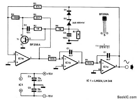
The frequency of the generator is determined by integrators IC1B and IC1C. An integrator has two properties that are used in this design. Firstly, a phase shift of 90° is between the input and output (ignor-ing, for the moment, the nonideal behavior of the op amp), and secondly, its amplification is - 1 (i.e., the signal inverts), provided the frequency:Cascading two identical integrators will thus result in an overall phase shift of 180° and an amplification of unity (provided that the frequency is1/2π/R1C1): an ideal basis for art oscillator. The two integrators are connected in the feedback circuit of an amplifier whose gain is determined by the amplitude of the output signal. Consequently, the generator has reasonably stable output voltage (at a level of about 4.5 Vpp).With the values of C1 (C1') and RI (R1'), as shown in the diagram, the output has a frequency of about 300 Hz. The frequency can be varied by replacing R1and R1' with a stereo potentiometer. To keep the frequency setting within bounds, the overall range of this potentiometer should not exceed a decade.The maximum attainable frequency is about 5 kHz. Distortion is not greater than 0.10/0. The current drawn by the generator is only a few milliamperes. Finally, the LM348 is a quadruple 741; it is thus possi-ble to construct the generator from four 741s. (View)
View full Circuit Diagram | Comments | Reading(1545)
SIGNAL_POWERED_RECEIVER
Published:2009/7/19 23:36:00 Author:Jessie
Circuit receives and reclines r-f radiation, stores resultant d-c energy in C2, and releases energy to transistors as required. Unique dipole rectifier provides efficient antenna-to-receiver coupling for frequencies of above 50 Mc.-L. It. Crump, Radio Waves Power Transistor Circuits, Electronics, 31:19, p 63-65. (View)
View full Circuit Diagram | Comments | Reading(699)
STABLE_40_MC_OSCILLATOR
Published:2009/7/19 23:36:00 Author:Jessie
Frequency shifts less than 500 kc when supply voltage is changed from 5 to 12 V.-T. P. Prouty, Using Varactors to Extend Frequency-Control Range, Electronics, 36:45, p 48-49. (View)
View full Circuit Diagram | Comments | Reading(766)
VARICAP_TUNES_TUNNEL_DIODE_OSCILLATOR
Published:2009/7/19 23:35:00 Author:Jessie
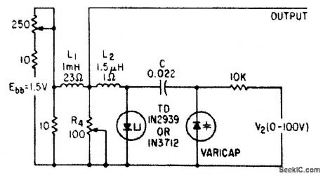
Series oscillator circuit tunes electrically over range of 12 to 22 Mc.-E. Gottlieb and J. Giorgis, Tunnel Diodes-Using Them as Sinusoidal Generators, Electronics, 36:24, p 36-42. (View)
View full Circuit Diagram | Comments | Reading(1917)
AUTOMATIC_LEVEL_CONTROL_FOR_PARAMETRIC_MAPLIFIER
Published:2009/7/19 23:35:00 Author:Jessie
Varactor diode in pump feed line feeds so-called magnifies d-c amplifier that in turn drives ferrite variable attenuator, to hold troposcatter receiver signal level constant over entire klystron mode.-W.L. Smott and H. C. Leahy, Parametric Amplifier Improves Tropo-Scatter System, Electronics, 35:9, p 38-40. (View)
View full Circuit Diagram | Comments | Reading(1345)
DAMPED_40_MC_GENERATOR
Published:2009/7/19 23:34:00 Author:Jessie
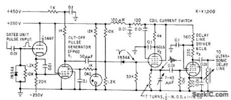
Converts unit pulses, resulting from video screening in nuclear track scanner, to damped 40-Mc oscillations each 0.1 microsec long, which are inserted in quartz ultrasonic delay line that feeds counter.-P. V. C. Hough, J. A Koenig, and W. Williams, Scanner Recognizes Atomic Particle Tracks, Electronics, 32:13, p 58-61. (View)
View full Circuit Diagram | Comments | Reading(815)
| Pages:86/195 At 2081828384858687888990919293949596979899100Under 20 |
Circuit Categories
power supply circuit
Amplifier Circuit
Basic Circuit
LED and Light Circuit
Sensor Circuit
Signal Processing
Electrical Equipment Circuit
Control Circuit
Remote Control Circuit
A/D-D/A Converter Circuit
Audio Circuit
Measuring and Test Circuit
Communication Circuit
Computer-Related Circuit
555 Circuit
Automotive Circuit
Repairing Circuit