
Signal Processing
Index 97
3_digit_ISUP2_SUPL_DPM_with_Beckman_gas_discharge_display
Published:2009/7/20 22:19:00 Author:Jessie
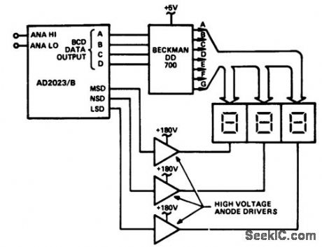
3-digit I2L DPM with Beckman gas discharge display (courtesy Analog Devices, Inc.). (View)
View full Circuit Diagram | Comments | Reading(715)
Programmable_function_generator_with_square_and_triangular_wave_outputs
Published:2009/7/20 22:19:00 Author:Jessie
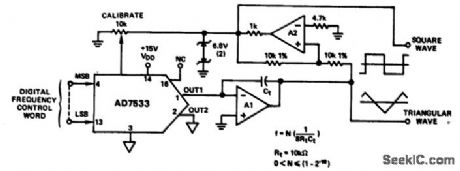
Programmable function generator with square and triangular wave outputs (courtesy Analog Devices, Inc.). (View)
View full Circuit Diagram | Comments | Reading(748)
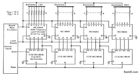
12_digit_CMOS_gas_discharge_display_
Published:2009/7/20 22:18:00 Author:Jessie
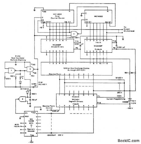
12-digit CMOS gas discharge display (courtesy Motorola Semiconductor Products Inc.). (View)
View full Circuit Diagram | Comments | Reading(639)
Staircase_generator
Published:2009/7/20 22:18:00 Author:Jessie
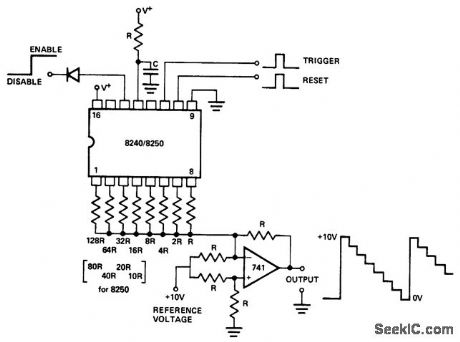
Staircase generator. The resistor array is switched to ground to generate binary or BCD weighted currents. The op amp converts these currents to an output voltage. Under reset condition the switches are off and the output is at ground. When a trigger is applied the output goes to VREF and generates a negative-going staircase of 256 levels for the 8240 or 100 level for the 8250. The time duration of each step is equal to the time base period, T = RC. The amplitude of the staircase can be varied by changing the input reference voltage. The stair-case can be stopped at any desired level by applying a disable signal to pin 14 (courtesy Intersil, Inc.). (View)
View full Circuit Diagram | Comments | Reading(0)
4_digit_direct_drive_LCD
Published:2009/7/20 22:11:00 Author:Jessie
4-digit direct drive LCD (courtesy Motorola Semiconductor Products Inc.). (View)
View full Circuit Diagram | Comments | Reading(0)
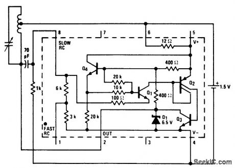
Space_mark_generator_with_voltage_controlled_duty_cycle
Published:2009/7/20 22:09:00 Author:Jessie
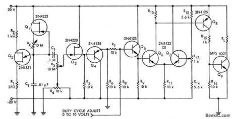
Space mark generator with voltage-controlled duty cycle. Frequency is set by RE in the source circuit of Q1 (courtesy Motorola Semiconductor Products Inc.). (View)
View full Circuit Diagram | Comments | Reading(779)
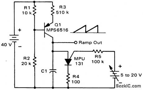
Sawtooth_generator_with_negative_going_ramp_using_a_zener_and_a_PNPN_diode
Published:2009/7/20 22:06:00 Author:Jessie
Sawtooth generator with negative-going ramp using a zener and a PNPN diode (courtesy Motorola Semiconductor Products Inc.). (View)
View full Circuit Diagram | Comments | Reading(1126)
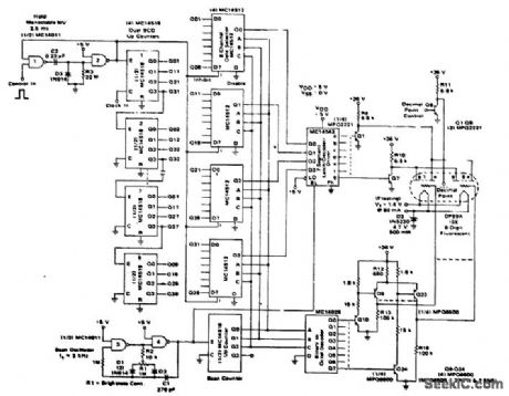
Real_time_5_digit_fluorescent_diode_display
Published:2009/7/20 22:33:00 Author:Jessie
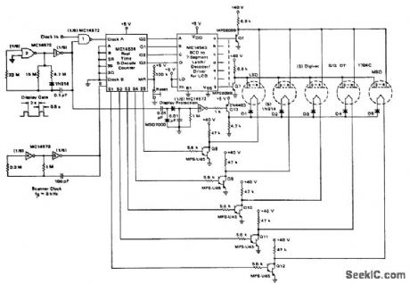
Real-time 5-digit fluorescent diode display(courtesy Motorola Semiconductor Products Inc.). (View)
View full Circuit Diagram | Comments | Reading(885)
Voltage_controlled_ramp_generator_VCRG_using_a_PUT
Published:2009/7/20 22:31:00 Author:Jessie
Voltage-controlled ramp generator (VCRG) using a PUT. Setting the value of C to 0.0047 μF provides a change in frequency of 3.4 ms; setting it to 0.01 μF provides a change of 5.4 ms (courtesy Motorola Semiconductor Products Inc.). (View)
View full Circuit Diagram | Comments | Reading(945)
8_digit_fluorescent_triode_display
Published:2009/7/20 22:29:00 Author:Jessie
8-digit fluorescent triode display (courtesy Motorola Semiconductor Products Inc.). (View)
View full Circuit Diagram | Comments | Reading(1074)
Staircase_generator_1
Published:2009/7/20 22:28:00 Author:Jessie
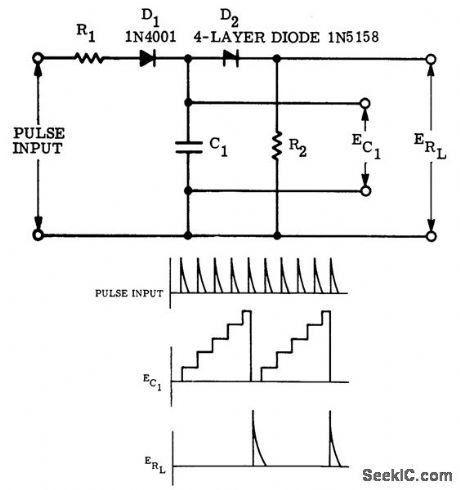
Staircase generator. The number of steps is determined as follows: h = (11RLVBR)/[(Vp - VBR)tp], where n is the number of steps, VBR is the break-down voltage of the PNPN diode, VP is the peak pulse with and tp is the pulse width (courtesy Motorola Semiconductor Products Inc.). (View)
View full Circuit Diagram | Comments | Reading(1041)
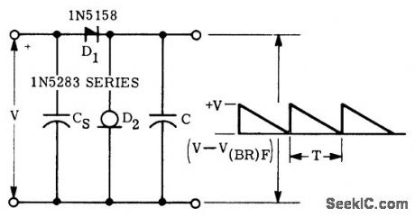
Staircase_generator_2
Published:2009/7/20 22:43:00 Author:Jessie
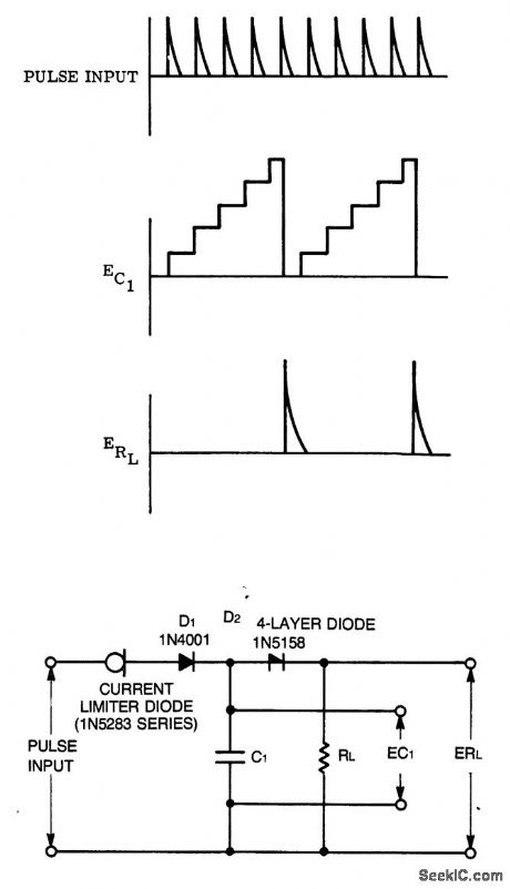
Staircase generator. The number of steps is determined as follows: n=(C1 VBR)/(Iptp), where n is the number of steps, VBR is the breakdown voltage at the PNPN diode, IP is the pinchoff voltage of the 1N5283 and tp is the pulse width (courtesy Motorola Semiconductor Products Inc.). (View)
View full Circuit Diagram | Comments | Reading(717)
Precision_ramp_generators_using_a_Datel_ADC_MC8B_16_pin_DIP
Published:2009/7/20 22:39:00 Author:Jessie
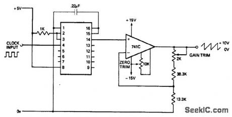
Precision ramp generators using a Datel ADC-MC8B 16-pin DIP. Pin functions of the ADC-MC8B are as follows: pin 1, ground; pin 2, logic select; pin 3, reset; Pin 4, strobe; pin5, bit8(LSB); pin6, bit7; pin 7, bit6; pin8, +Vcc; pin 9, bit 5; pin 10, bit4; pin 11, bit3; pin 12, bit2; pin 13, bit 1 (MSB); pin 14, analog output; pin 15, VREF input; pin 16, VREF output (courtesy Datel Systems, Inc.). (View)
View full Circuit Diagram | Comments | Reading(658)
Single_pulse_generator_using_an_SUS
Published:2009/7/20 22:37:00 Author:Jessie
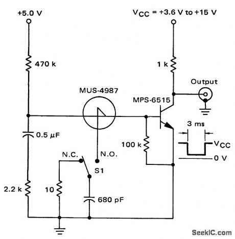
Single pulse generator using an SUS. This circuit is useful in testing digital equipment. The output is a clean debounced pulse of 3 ms duration (courtesy Motorola Semiconductor Products Inc.). (View)
View full Circuit Diagram | Comments | Reading(803)
1_MHz_oscillator_using_the_MC1553_video_amplifier
Published:2009/7/20 23:06:00 Author:Jessie
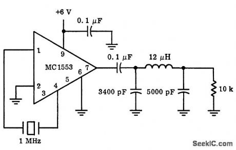
1 MHz oscillator using the MC1553 video amplifier (courtesy Motorola Semiconductor Products Inc.). (View)
View full Circuit Diagram | Comments | Reading(618)
27_MHz_transmitter_for_CB_operation
Published:2009/7/20 23:05:00 Author:Jessie
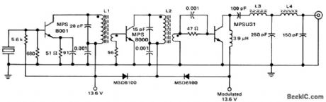
27 MHz transmitter for CB operation. Power output is 3.5 watts minimum. Typical efficiency is 70%. Modulation can be±100%. Second harmonic suppression istypically 38 dB down, while third harmonicsuppression is 55 dB down. All coilsare on 1/4-inch forms with AWG #22 wire. Slugs are 1/4 by 3/8-inch J-types. Secondary windings are overwound on the bottom of the primary. L1 primary is 12 turns close wound, while the secondary is 2 turns. L2 primary is 18 turns close wound, while its secondary is 2 turns. L3 is 7 turns dose wound. L4 is 5 turns close wound (courtesy Motorola Semiconductor Products Inc.). (View)
View full Circuit Diagram | Comments | Reading(2710)
Variable_audio_oscillator_with_a_range_of_20_hertz_to_20_kilohertz
Published:2009/7/20 23:04:00 Author:Jessie
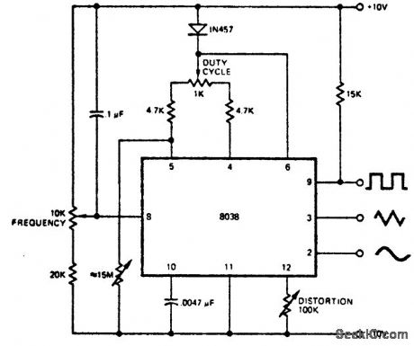
Variable audio oscillator with a range of 20 hertz to 20 kilohertz. The chip used is an Intersil 8038 waveform generator, which is a 14-pin DIP (courtesy Intersil, Inc.). (View)
View full Circuit Diagram | Comments | Reading(2121)
800_kHz_experimental_BF_oscillator_using_an_LM3909_chip
Published:2009/7/20 23:03:00 Author:Jessie
800 kHz experimental BF oscillator using an LM3909 chip. Circuitry inside the dashed lines is the LM3909. The external coil is a standard broadcast loopstick. The variable capacitor is 360 pF (courtesy National Semiconductor Corporation). (View)
View full Circuit Diagram | Comments | Reading(620)
Crystal_oscillator_with_amplitude_modulated_output
Published:2009/7/20 23:01:00 Author:Jessie
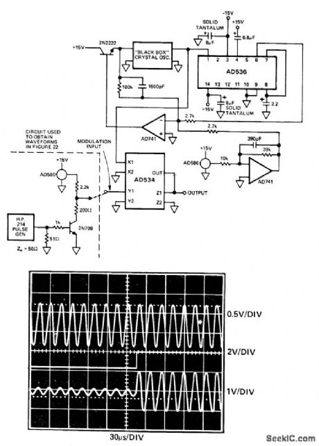
Crystal oscillator with amplitude-modulated output. The black box crystal oscillator output is converted to DC by the AD536 PMS/DC converter. The AD536 output is summed in the AD741 with the DC reference voltage obtained by inverting and amplifying the output of the AD580 band-gap reference. The AD741 drives the 2N2222 control transistor to close the feedback loop around the oscillator by adjusting its supply voltage. The AD534 serves as an amplitude modulator. The oscilloscope waveforms show the 32.768 kHz signal being switched by a fast step from 0.3 to 2.2 volts peak to peak with no ringing, overshoot, etc. (courtesy Analog Devices, Inc.). (View)
View full Circuit Diagram | Comments | Reading(1216)
Low_distortion_oscillator
Published:2009/7/20 22:58:00 Author:Jessie
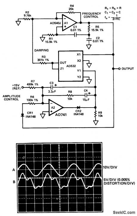
Low-distortion oscillator. A1 is connected as a noninverting amplifier and has again of three. As shown the oscillator output is 1 kHz, determined by R1, R5, C1 and C2. See equation in diagram to determine frequency (courtesy Analog Devices, Inc.). (View)
View full Circuit Diagram | Comments | Reading(2562)
| Pages:97/195 At 2081828384858687888990919293949596979899100Under 20 |
Circuit Categories
power supply circuit
Amplifier Circuit
Basic Circuit
LED and Light Circuit
Sensor Circuit
Signal Processing
Electrical Equipment Circuit
Control Circuit
Remote Control Circuit
A/D-D/A Converter Circuit
Audio Circuit
Measuring and Test Circuit
Communication Circuit
Computer-Related Circuit
555 Circuit
Automotive Circuit
Repairing Circuit