
Signal Processing
Index 91
WAVEFORM_GENERATOR_STABLE_VCO
Published:2009/7/9 3:49:00 Author:May
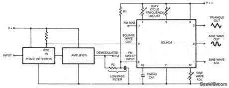
In this circuit, a waveform generator is used as a stable VCO in a Phase-Locked Loop (PLL). (View)
View full Circuit Diagram | Comments | Reading(1236)
ALLOPHONE_GENERATOR
Published:2009/7/9 3:40:00 Author:May
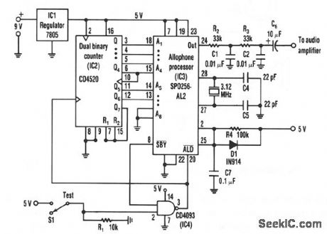
The circuit, a general-purpose system with many uses, vocalizes 59 allophones contained in the speech processor. After filtering and amplification, its pulse-code-modulated output can drive an 8-Ω speaker. The processor's address pins, A1 to A6, define 64 speech-entry points.Closing the test switch to the NAND gate lowers its output, thereby loading an address and triggering the ALD input for an allophone cycle. The CD4520 dual binary counter, IC2, counts from 0 to 63 in binary code until its Q7 output resets it on the number 64 count. To generate a phrase, just add an EPROM between IC2 and IC3 that contains a program for a predetermined sequence of allophones. (View)
View full Circuit Diagram | Comments | Reading(1227)
COMPUTER_SPEECH_SYNTHESIZER
Published:2009/7/9 3:25:00 Author:May
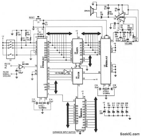
This text-to-speech converter is built around the SPO256-AL2 speech processor and the CT6256-AL2 text-to-speech converter chips-manufactured by General Instruments. The circuit is set up to receive standard ASCII code from virtually any microcomputer or dumb terminal that is equipped with an RS-232 port-such as a serial-printer or modem port. If a microcomputer is used, the synthesizer can be activated from a terminal-emulator of any communications proaram, or front any programming language such as BASIC.The serial input from the RS-232 port enters the circuit through U7, the MC1489 RS-232 receiver chip, and is converted from an RS-232 level to a TTL-level signal. The CTS256-AL2 chip, U1, then converts the ASCII characters into allophone codes and sends those codes to U3, the TMS4016 external-RAM chip. The codes are then transferred to the SPO256-AL2, U2, through the 74LS373 octal latch, U4. Finally, the SPO256-AL2 sends out an audio signal to the LM386 audio amplifier, U8, through some highpass filtering, and on to the speaker. The 74LS138d, US, and the 74LSO4, U6, provide control logic. (View)
View full Circuit Diagram | Comments | Reading(3302)
COLOR_TV_CROSSHATCH_GENERATOR
Published:2009/7/9 2:53:00 Author:May
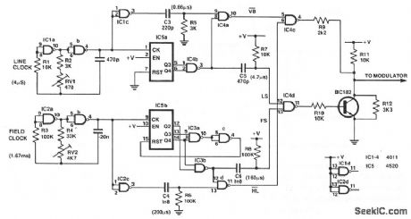
This circuit provides a simple, low-cost crosshatch generator tor convergence and geometry adjustments on color TVs. The generator is driven by two clocks, one for the horizontal drive, IC1ab, and one for the vertical drive, IC2ab. The clock outputs are applied to the two binary counters contained in IC5 which generate the line and field sync pulses and respective blanking periods. Line clock pulses, buffered by IClc, are differentiated by C3/R5 to produce the vertical bars. These bars are gated by IC4a which suppresses the bars during the line blanking period produced by the coincidence of Q3, Q4 outputs of IC5a, detected by IC4b. This output is also differentiated by C5/R7 to produce the line sync pulse, LS. A similar process is used to generate horizontal lines and the field sync, except that in order to give the correct aspect ratio, the count of IC5b is reset at 12, coincidence of Q3 and Q4. In coincidence of Q2, Q4 is used to generate the sync pulse FS and the blanking period. The line and field sync pulses, LS and FS, are combined in IC4d. (View)
View full Circuit Diagram | Comments | Reading(1736)
TWO_STAGE_SOLID_STATE_VIDEO_AMPLIFIER
Published:2009/7/20 20:39:00 Author:Jessie
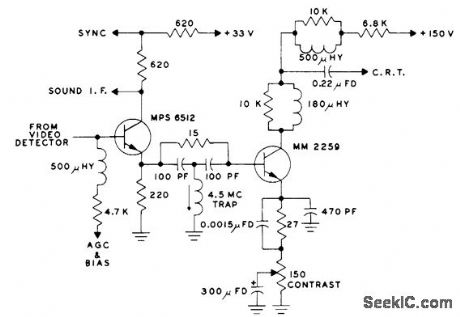
Provides cathode drive for crt of tv receiver, along with sync takeoff from driver. Driver also serves as sync amplifier, first sound amplifier, and keyer for agc stage. -D, L, Wollensen, Solid-State Television Video Amplifiers, Motorola Application Note AN-165, Doc. 1965.
(View)
View full Circuit Diagram | Comments | Reading(743)
HORIZONTAL_SYNC_TRANSIENT_DISPLAY
Published:2009/7/20 20:38:00 Author:Jessie
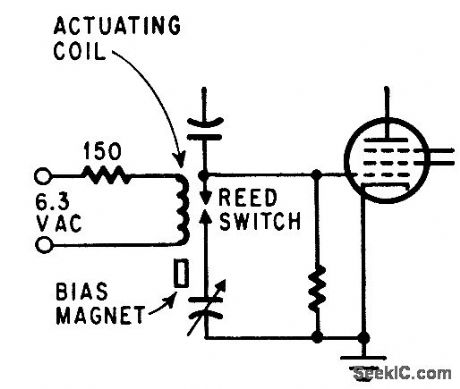
Reed switch operated at field frequency from ac heater voltage, with permanent magnet providing magnetic bias to get 60 cps, permits observing single transient continuously while making tv receiver circuit adjustment. -M. B. Knight, Reed Switches for Breadboarding, Electronics, 37:16, p 93 (View)
View full Circuit Diagram | Comments | Reading(743)
The heating magnetic mixer (2)
Published:2011/7/21 21:58:00 Author:qqtang | Keyword: heating magnetic mixer
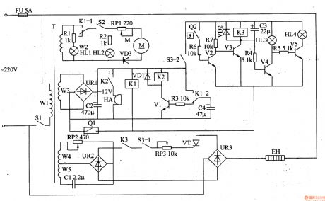
Here is to introduce the heating magnetic mixer which has the functions of stepless speed regulation mixing, constant temperature auto control, stepless temperature regulation and timing alarm, etc, it can be used in the labs chemical and steel area.The working principle of the circuit The heating magnetic mixer consists of the power supply circuit, mixing motor control circuit, heating temperature regulation circuit, mixing circuit motor speed regulation circuit, timing alarm circuit and timing control circuit, see as figure 8-139.
(View)
View full Circuit Diagram | Comments | Reading(754)
AUTOMATIC_LOCAL_FRINGE_TUNING
Published:2009/7/20 20:28:00 Author:Jessie
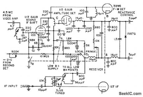
Complele automatic fine tuning system com bines features of fringe switching and auto matic-manual operation. Switching transients are reduced by 180-mmfd capacitor-C. W. Baugh, Jr., and L. J. Sienkiewicz, Sound Signal Tunes Tv Automatically, Electronics, 31:17, p 54-58. (View)
View full Circuit Diagram | Comments | Reading(759)
65_240_Hz
Published:2009/7/20 19:57:00 Author:Jessie
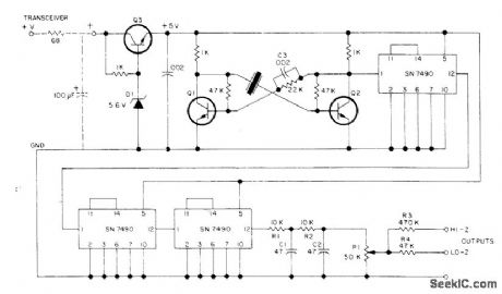
Output of 65-240 kHz crystal oscillator is divided by 1000 in three SN7490s to give 65-240 Hz tone required for access to amateur FM repeater. Choose crystal to give exactly desired frequency Q1 and Q2 are MPS6513, and Q3 is 2N1613. Supply can be 9 to 15 VDC from transceiver or from 9-V battery.-P. H. Wiese, Rock Solid Subaudible Tone Generator, 73 Magazine, April 1974, p 79-81. (View)
View full Circuit Diagram | Comments | Reading(823)
OSCILLOSCOPE_COUNTER_PREAMPLIFIER
Published:2009/7/9 2:04:00 Author:May
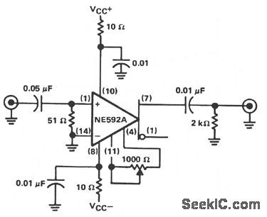
The circuit will provide a 20±0.1 dB voltage gain from 500 kHz to 50 MHz. The low-frequency response of the amplifter can be extended by increasing the value of the 0.05-μF capacitor connected in series with the input terminal. This circuit will yield an input-noise level of approximately 10 μV over a 1 5. 7-MHz bandwidth. The gain can be catibrated by adjusting the potentiometer connected between pins 4 and 11. The 1-KΩ potentiometer can be adjusted for an exact voltage gain of 10. This preserves the scale factor of the instrument. (View)
View full Circuit Diagram | Comments | Reading(905)
OSCILLOSCOPE_CALIBRATOR
Published:2009/7/9 1:59:00 Author:May
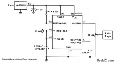
The calibrator can be used to check the accuracy of a time-base generator, as well as to calibrate the input level of amplifiers. The calibrator consists of an NE555 connected in the astable mode. The oscillator is set to exactly 1 kHz by adjusting potentiometer P1 while the output at pin 3 is being monitored against a known frequency standard or frequency counter. The output level, likewise, is monitored from potentiometer P2's center arm to ground with a standard instrument. P2 is adjusted for 1 V pk-pk at the calibrator output terminal. During operation, the calibrator output terminal will produce a 1-kHz, square-wave signal at 1 V pk-pk with about 50% duty cycle. For long-term oscillator frequency stability, C1 should be a low-leakage mylar capacitor. (View)
View full Circuit Diagram | Comments | Reading(1019)
LOW_VOLTAGE_WIEN_BRIDGE_OSCILLATOR
Published:2009/7/9 1:52:00 Author:May
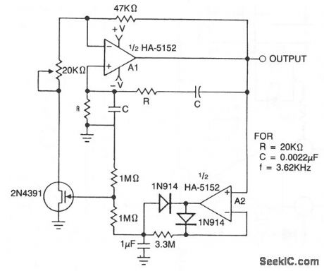
This circuit utilizes an HA-5152 dual op amp and FET to produce a low-voltage, low-power, Weinbridge sine-wave oscillator. Resistors R and capacitors C control the frequency of oscillation; the FET, used as a voltage-controlled resistor, maintains the gain of A1 exactly 3 dB to sustain oscillation. The 20-KΩ pot can be used to vary the signal amplitude. The HA-5152 has the capability to operate from ±1.5-V supplies. This circuit will produce a low-distortion sine-wave output while drawing only 400 uA of supply current.
(View)
View full Circuit Diagram | Comments | Reading(1232)
PUNCHED_TAPE_READER
Published:2009/7/20 7:39:00 Author:Jessie
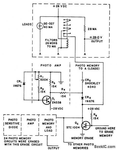
Uses photo memory to drive loads, to keep signal applied to load until memory is erased. Lamp load can be used for verifying punched paper tape. Relay load controls circuit where it is necessary to handle large currents. Relay used exceeds continuous rating of CR2, so one set of relay contacts keeps relay latched. Resistive load is used to drive logic circuits. Sensor can be either photodiode or standard 1N676 diode with paint removed from glass case. -Photo Reader for Perforated Tape, Electronic Circuit Design Handbook, Mactier Pub. Corp., N.Y., 1965, p 207. (View)
View full Circuit Diagram | Comments | Reading(0)
5_V_OSCILLATOR
Published:2009/7/9 1:51:00 Author:May
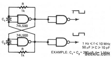

Consistently self-starting and yet capable of operating from over 1 Hz to 10 MHz, this low-cost oscillator requires only five components. Calculate the period of oscillation by using this relationship: P = 5 ×10³ C sec when C= C1=C2. Bychanging the ratio of C1 to C2, the duty cycle can be as low as 20%. (View)
View full Circuit Diagram | Comments | Reading(1101)
PRECISION_VOLTAGE_CONTROLLED_OSCILLATOR
Published:2009/7/9 1:50:00 Author:May
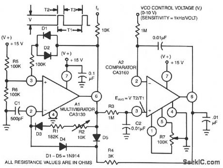
This circuit uses a CA3130 BiMOS op amp as a multivibrator and CA3160 BiMOS op amp as a com-parator. The oscillator has a sensitivity of 1 kHz/V, with a tracking error in the order of 0.02%, and a temperature coefficient of 0.01%℃. (View)
View full Circuit Diagram | Comments | Reading(0)
CODE_PRACTICE_OSCILLATOR
Published:2009/7/9 1:49:00 Author:May
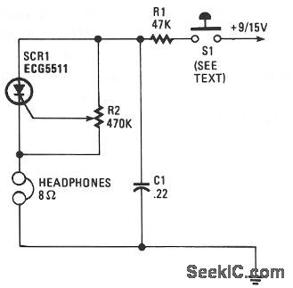
Capacitor C1 charges through resistor R1, and when the gate level established by potentiometer R2 is high enough, the SCR is triggered. Current flows through the SCR and earphones, discharging C1. The anode voltage and current drop to a low level, so the SCR stops conducting and the cycle is repeated. Resistor R2 lets the gate potential across C1 be adjusted, which charges the frequency or tone. Use a pair of 8-Ω headphones. The telegraph key goes right into the B+ line, 9-V battery. (View)
View full Circuit Diagram | Comments | Reading(0)
CMOS_OSCILLATOR_1
Published:2009/7/9 1:48:00 Author:May
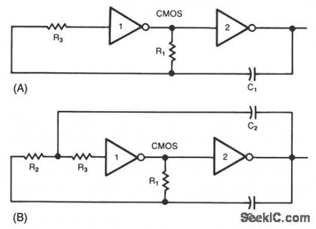
The common clock oscillator in Fig. 68-19A has two small problems: It might not, in fact, oscil-late if the transition regions of its two gates differ. If it does oscillate, it might sometimes oscillate at a slightly lower frequency than its equation predicts because of the fmite gain of the ftrst gate. If the circuit does work, oscillation occurs usually because both gates are in the package and, therefore, have logic thresholds only a few millivolts apart.
The circuit in Fig. 68-19B resolves both prob-lems by adding a resistor and a capacitor. The R2/ C2 network provides hysteresis, thus delaying the onset of gate 1's transition until C1 has enough voltage to move gate 1 securely through its transi-tion region. When gate 1 is finally in its transition region, C2 provides positive feedback, thus rapidly moving gate 1 out of its transition region.
The equations for the oscillator in Fig. 68-19B are:
(View)
View full Circuit Diagram | Comments | Reading(949)
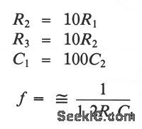
XOR_GATE_OSCILLATOR
Published:2009/7/9 1:44:00 Author:May
An exclusive-OR gate, IC1D, turns a simple CMOS oscillator into an FSK generator. When the data input increases, IC1D inverts, and negative feedback through R2 lowers the circuit's output frequency. A low input results in positive feedback and a higher output frequency. R1 and C set the oscillator's frequency range, and R2 determines the circuit's frequency shift. To ensure frequency stability, make R3 much greater than R1 and use a high-quality feedback capacitor. The three gates constituting the oscillator itself need not be exclusive-OR types; use any CMOS inverter. (View)
View full Circuit Diagram | Comments | Reading(1453)
CMOS_OSCILLATOR
Published:2009/7/9 1:43:00 Author:May
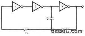
This circuit is guaranteed to oscillate at a frequency of about 2.2/(R1 ×C) if R2 is greater than R1 You can reduce the number of gates further if you replace gates 1 and 2 with a noninverting gate. (View)
View full Circuit Diagram | Comments | Reading(0)
WIEN_BRIDGE_OSCILLATOR
Published:2009/7/9 1:42:00 Author:May
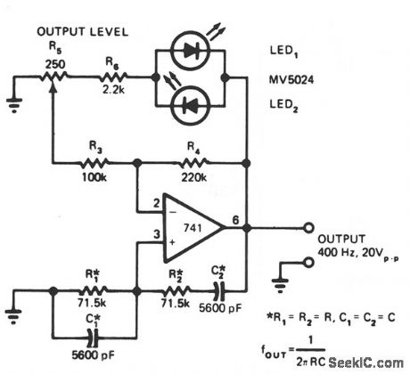
LEDs function as both pilot lamps and as an AGC (automatic gain control) in this unconventional amplitude-stabilized oscillator. (View)
View full Circuit Diagram | Comments | Reading(0)
| Pages:91/195 At 2081828384858687888990919293949596979899100Under 20 |
Circuit Categories
power supply circuit
Amplifier Circuit
Basic Circuit
LED and Light Circuit
Sensor Circuit
Signal Processing
Electrical Equipment Circuit
Control Circuit
Remote Control Circuit
A/D-D/A Converter Circuit
Audio Circuit
Measuring and Test Circuit
Communication Circuit
Computer-Related Circuit
555 Circuit
Automotive Circuit
Repairing Circuit