
Signal Processing
Index 96
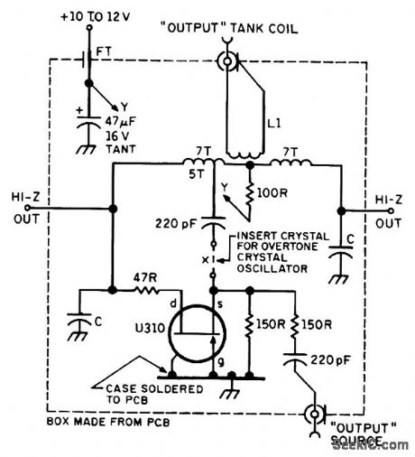
STABLE_INDUCTIVE_TUNED_OSCILLATOR
Published:2009/7/21 2:56:00 Author:Jessie

In frequency-shift keying (FSK) applications, when modulating high data rates, coupling data to the varactor can pose a problem. A duplex filter is necessary to prevent RF loading or leaking of the oscillator tank while transferring the fast data edges to the varactor. These two constraints contradict one another-especially when the edge's rise time approaches that of the carrier frequency. If an RF choke or a large-value resistor is used to inject data to the varactor, then the edges of the data will be severely distorted by RC or inductive-capacitive (LC) time constants. The loss of these rise times can result in duty-cycle distortion as seen by the threshold level detector in the receiver. To improve upon the traditional VCO techniques, varying the inductor provides increased tuning sensitivity and better resonator Q. Inductive tuning uses the coupling or leakage inductance characteristics of a transformer. Thus, tuning capacitor C4 can be changed to a fixed, high-quality capacitor. Use of a negative -temperature -coefficient capacitor here can balance out the active device's capacitance variation with temperature. The tuning inductor (L1) is now a transformer. At about 48 MHz, it is a nine-turn, center-tapped coil of AWG28 wound on a 725-10 Micrometals core. Other transformers also can be implemented, depending on operating frequencies and performance requirements. The Q for this inductor is about 100, which is more than sufficient to isolate the active device to prevent its pulling the oscillator tank over the extended temperature range of -40 to 85℃. The inductance variation or stability with temperature is dependent on the core material of L1. (View)
View full Circuit Diagram | Comments | Reading(1165)
LOW_NOISE_OSCILLATOR
Published:2009/7/21 2:57:00 Author:Jessie
This oscillator is suitable for low-noise applications. L is wound on a 6-mm form, and C is 15 to 220 pF. The frequency range is 20 to 80 MHz. The output is 0 dBm into 50 Ω. For use of the circuit as a crystal-controlled oscillator, a crystal can be inserted as shown. (View)
View full Circuit Diagram | Comments | Reading(870)
Vector_magnitude_function_from_the_4301_multifunction_chip
Published:2009/7/21 2:57:00 Author:Jessie
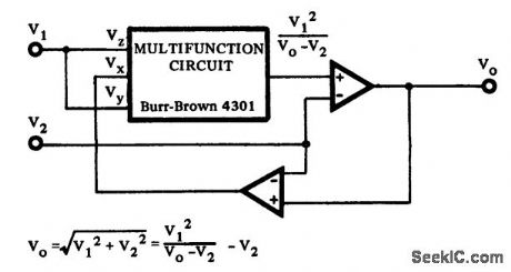
Vector magnitude function from the 4301 multifunction chip (courtesy Burr-Brown Research Corporation). (View)
View full Circuit Diagram | Comments | Reading(568)
TTL_RING_OSCILLATOR
Published:2009/7/21 2:58:00 Author:Jessie
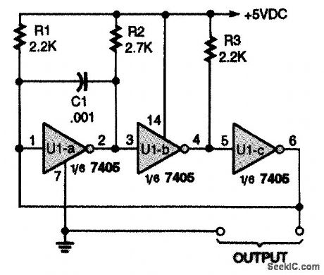
A TTL ring-oscillator circuit uses an odd number of inverters in an astable configuration. (View)
View full Circuit Diagram | Comments | Reading(924)
FRANKLIN_OSCILLATOR
Published:2009/7/21 2:59:00 Author:Jessie

Shown in tube form, this circuit shows the principle and the configuration of the Franklin oscillator.
The basic Franklin master oscillator, first described in 1930, uses very low-value capacitors, C1 and C2 (about 1 to 3 pF), imposing a very light load on the high-Q tuned circuit. Further advantages include the two-terminal inductance and the earthing of one end of the resonant circuit. This form of oscillator can be readily adapted for use with MOSFET devices. (View)
View full Circuit Diagram | Comments | Reading(2395)
CENTER_TAPPED_TRANSFORMER_AUDIO_OSCILLATOR
Published:2009/7/21 2:03:00 Author:Jessie
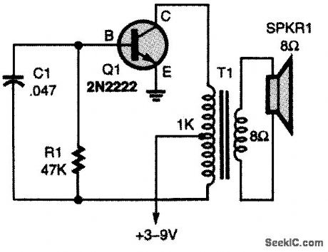
The oscillator circuit uses a center-tapped transistor output transformer to serve as a load for the collector of Q1, supply a feedback signal for the base, and serve as the output winding for driving the speaker. R1 supplies dc bias and C1 completes the ac path from the transformer to Q1's base. You can play around with the values of C1 and R1 to change the oscillator's output level and tone, but don't reduce R1's value too much or the transistor will draw excessive collector current. (View)
View full Circuit Diagram | Comments | Reading(3737)
Difference_of_squares_circuit
Published:2009/7/21 2:04:00 Author:Jessie
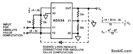
Difference-of-squares circuit. This circuit computes the difference of the squares of two input signals. It is useful in vector computations and in weighing the difference of two magnitudes to emphasize the greater nonlinearity. It can also be used to determine absolute value if A is the input, B is connected to EO through a diode and both Z terminals are grounded (courtesy Analog Devices, Inc.). (View)
View full Circuit Diagram | Comments | Reading(701)
SIX_RANGE_RF
Published:2009/7/21 2:04:00 Author:Jessie
Covers from 100 kHz to about 75 MHz in six bands, for checking low-frequency IF circuits on up to VHF circuits (using harmonics up to 220 MHz). Omission of frequency read-out dial scale simplifies design without affecting usefulness for troubleshooting. FETs can be HEP-802 or MPF102, and output transistor is 2N3866 or 2N706, First FET is Hartley oscillator lightly coupled through 5-pF capacitor to FET source-follower isolation stage. Last stage boosts signal level up to about 1 V on most bands. Tuning capacitor is broadcast-band type having 300-pF AM section and 25-pF FM section. Set of six coils can be purchased as Conar CO-69 through CO-74 from National Radio Institute or can be wound as suggested in article to give high-end band limits of 0.57, 1.4, 4.5, 17, 39, and 75-80 MHz. For portable use, 12-V battery pack or 9-V transistor radio battery can be used to give constant 9-V supply.-Brew Up a Signal Generator, 73Magazine, Jan. 1978, p 50-52. (View)
View full Circuit Diagram | Comments | Reading(949)
30_Hz_TO_100_kHz
Published:2009/7/21 2:06:00 Author:Jessie
Wien-bridge sine-wave oscillator using two RCA CA3140 opamps covers frequency range with less than 0.5% total harmonic distortion. Adjust 10K pot for best output waveform. Maximum output into 600-ohm load is about 1 VRMS. Opamps are direct replacements for 741 but have higher input impedance and better slew rate.-C. Hall, New Op Amp Challenges the 741, Ham Radio, Jan. 1978, p 76-78. (View)
View full Circuit Diagram | Comments | Reading(816)
Precision_high_CMV_common_mode_voltage_analog_isolator
Published:2009/7/21 3:00:00 Author:Jessie
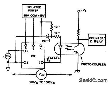
Precision high CMV (common mode voltage) analog isolator. This circuit provides up to 1500 volts DC CMV isolation. The V/F convener shown is a 452 with a full scale output of 100 kHz for 10 volts input (courtesy Analog Devices, Inc.). (View)
View full Circuit Diagram | Comments | Reading(856)
LOW_NOISE_DC_REGULATOR_FOR_OSCILLATOR_CIRCUITS
Published:2009/7/21 3:01:00 Author:Jessie
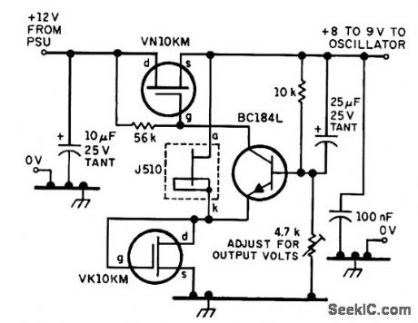
This regulator uses FET devices for low-noise dc output needed for use with variable-frequency free-running oscillators. (View)
View full Circuit Diagram | Comments | Reading(884)
SNS9201 (household appliance, robot, medical equipment or alarm device) infrared sensor signal processing circuit
Published:2011/8/1 8:42:00 Author:TaoXi | Keyword: household appliance, robot, medical equipment, alarm device, infrared sensor, signal processing
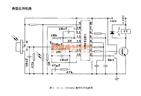
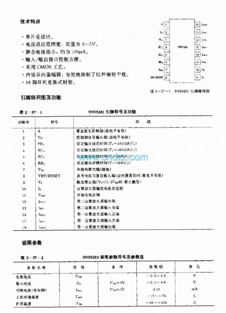

The SNS9201 is designed as the human body infrared sensor signal processing circuit that can be used in the household appliance, robot, medical equipment or alarm device applications. The internal circuit is composed of the linear amplifier circuit, the two-way limiter, the voltage comparator, the state controller, the reference power circuit, the signal processor, the delay timer and the blocking timing circuit.
Features
The monolithic design.The wide voltage range, the value is 3-5V.The quiescent current is small, it is about 100uA.The input/output port is easy to control.It uses the CMOS technology.It has the two-way amplitude discriminator.16-pin dual-row DIP package.
(View)
View full Circuit Diagram | Comments | Reading(1499)
S2559A/D/E/F general infrared remote control launch circuit (dual-tone multi-frequency signal generating circuit)
Published:2011/8/1 20:48:00 Author:TaoXi | Keyword: general, infrared, remote control, launch circuit, dual-tone, multi-frequency, signal generating

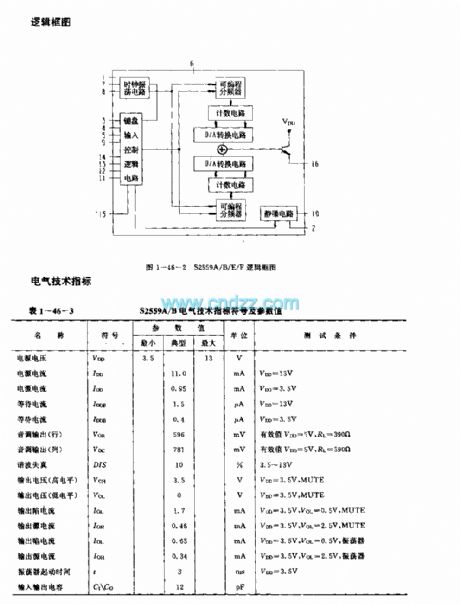
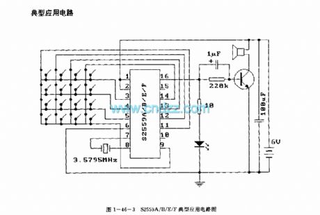
The S2559A/D/E/F is designed as the dual-tone multi-frequency signal generating circuit that can be used in the general infrared remote control launch circuit. The internal circuit is composed of the clock circuit, the keyboard input logic control circuit, the programmable frequency divider, the D/A converter circuit and the squelch circuit.
Features
The power supply voltage range is wide:3.5-13V(S2559A/B),2.5-10V(S2559E/F). The power consumption is small.The external crystal frequency is 3.579545MHz.The IC has the weak sound output.It is connected with the telephone keyboard directly.The harmonic distortion is small.Integrated circuit upstream oscillator resistor.The integrated circuit has the reference voltage.It can produce the single-tone.The static operating current is 0.4-1.5uA.The output driving current is 1-10mA.
(View)
View full Circuit Diagram | Comments | Reading(1907)
Modified_scale_factor_and_offset_circuit
Published:2009/7/21 4:36:00 Author:Jessie
Modified scale factor and offset circuit (courtesy Analog Devices, Inc.). (View)
View full Circuit Diagram | Comments | Reading(609)
Sine_function_generation_using_an_AD534_multiplier_divider_chip
Published:2009/7/20 22:16:00 Author:Jessie
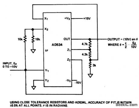
Sine function generation using an AD534 multiplier/divider chip (courtesy Analog Devices, Inc.). (View)
View full Circuit Diagram | Comments | Reading(639)
Frequency_synthesizer_using_an_external_time_base_reference
Published:2009/7/20 22:15:00 Author:Jessie
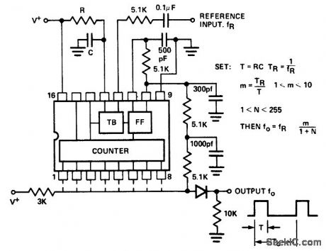
Frequency synthesizer using an external time base reference. The counter shown is an Intersil 8240 programmable timer/counter. The harmonic synchronization property of the 8240 time base can be used to generate a wide number of frequencies from a given input reference frequency (courtesy Intersil, Inc.). (View)
View full Circuit Diagram | Comments | Reading(715)
27_MHz_mixerfor_CB_operation_using_a_TIS148_dual_gate_MOSFET
Published:2009/7/20 22:15:00 Author:Jessie
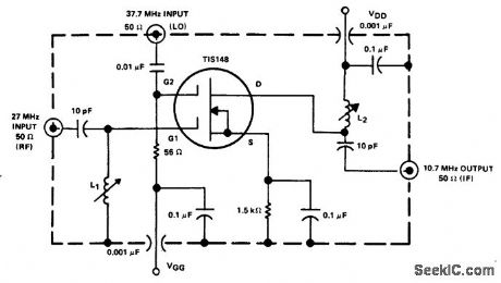
27 MHz mixerfor CB operation using a TIS148 dual-gate MOSFET (courtesy Texas Instruments Incorporated). (View)
View full Circuit Diagram | Comments | Reading(646)
Power_function_generator_developing_sine_wavestriangular_waves_and_square_waves
Published:2009/7/20 22:13:00 Author:Jessie
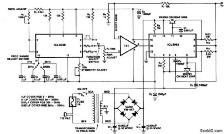
Power function generator developing sine waves,triangular waves and square waves. Operating frequency is 2 hertz to 20 kilohertz. VO is up to ±25 volts (50 volts peak to peak) across loads as small as 10 ohms, which produces a maximum of 2.5 amperes of output current. All capacitor working voltage ratings should be 50 volts DC. All resistors should be the half-watt type unless otherwise specified. Keep the lead at pin 2 of the op amp less than 2 inches or oscillations will result. Full power output is only obtainable up to about 5 kilohertz due to the op amp (courtesy Intersil, Inc.). (View)
View full Circuit Diagram | Comments | Reading(1615)
Sawtooth_generator_with_positive_going_ramp_using_a_zener_and_PNPN_diode
Published:2009/7/20 22:05:00 Author:Jessie
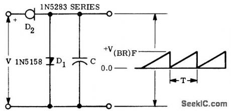
Sawtooth generator with positive-going ramp using a zener and PNPN diode (courtesy Motorola Semiconductor Products Inc.). (View)
View full Circuit Diagram | Comments | Reading(1292)
Programmable_triangle_square_wave_function_generator
Published:2009/7/20 21:58:00 Author:Jessie
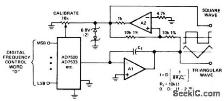
Programmable triangle/square-wave function generator. A1 and A2 are AD301 op amps. The peak-to-peak amplitude of both waveforms is approximately 15 volts (courtesy Analog Devices, Inc.). (View)
View full Circuit Diagram | Comments | Reading(710)
| Pages:96/195 At 2081828384858687888990919293949596979899100Under 20 |
Circuit Categories
power supply circuit
Amplifier Circuit
Basic Circuit
LED and Light Circuit
Sensor Circuit
Signal Processing
Electrical Equipment Circuit
Control Circuit
Remote Control Circuit
A/D-D/A Converter Circuit
Audio Circuit
Measuring and Test Circuit
Communication Circuit
Computer-Related Circuit
555 Circuit
Automotive Circuit
Repairing Circuit