
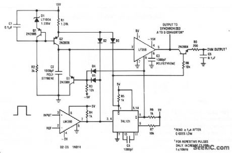
A/D-D/A Converter Circuit
Index 11
3_5_V_REGULATED_OUTPUT_CONVERTER
Published:2009/7/9 4:04:00 Author:May
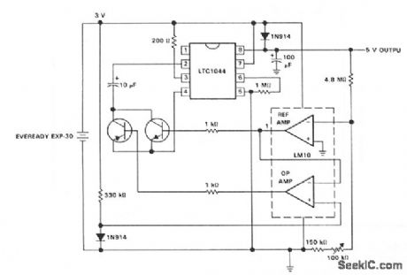
View full Circuit Diagram | Comments | Reading(905)
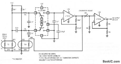
POTENTIOMETER_POSITION_V_F_CONVERTER
Published:2009/7/9 3:59:00 Author:May
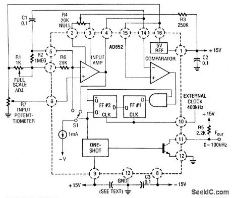
In this application, an AD652IC is used in a synchronized V/F converter that derives its input from the position of a potentiometer. This can represent a position of a mechanical component, weight, size, etc., to give a 0-to-100-kHz output versus the 0-to-5-V output from the potentiometer.
(View)
View full Circuit Diagram | Comments | Reading(1235)
5_V_TO_ISOLATED_5_V_AT_20_MA_CONVERTER
Published:2009/7/9 3:55:00 Author:May
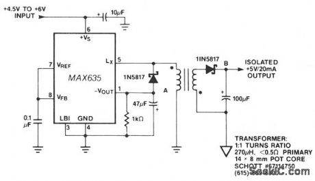
In this circuit, a negative output voltage dc-dc converter generates a -5 V output at pin A. In order to generate - 5 V at point A, the primary of the transformer must fly back to a diode drop more negative than -5 V. If the transformer has a tightly coupled 1/1 turns ratio, there will be a 5 V plus a diode drop across the secondary. The 1N5817 rectifies this secondary voltage to generate an isolated 5-V output. The isolated output is not fully regulated since only the -5 V at point A is sensed by the MAX635. (View)
View full Circuit Diagram | Comments | Reading(1787)
RGB_COMPOSITE_CONVERTER
Published:2009/7/9 1:56:00 Author:May
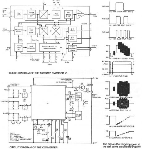
The incoming RGB inputs are terminated with resistors R1, R2, and R3 and potentiometers RV1, RV2, and RV3. These provide input impedances of approximately 750. The presets should be adjusted to provide a maximum input of 1 V pk-pk into the MC1377. The inputs are ac-coupled into the encoder; the large value capacitor is required for the 60 Hz field component.The Colpitts oscillator for the color burst is formed around pins 17 and 18. About 0.5 V pk-pk should appear on pin 17 and 0.25 V rms into pin 18 with the oscillator components removed. The incoming composite sync signal at pin 2 should be negative-going. The device will accept CMOS and TTL directly. If it is necessary to ac-couple the sync, then a pull-up to 8.2 V is required-a regulated 8.2 V is provided on pin 16.From the composite sync input, the MC1377 generates a ramp which it uses to provide the burst gate pulse. The slope of this ramp can be varied by a potentiometer on pin 1. However, a preset value, shown as 43 KΩ, is usually sufficient. The chrominance filter should be fitted between pins 13 and 10. If the filter is not used, a compensatory potential divider should be fitted (both are shown). We used a prealigned Toko bandpass filter centered on 4.43 MHz. If the chroma filter is fitted, the delay through it, 400 ns, has to be compensated for by a luminance delay line between pins 6 and 8. This line is shorted out if the filter is not fitted. The composite video output from the IC is buffered to provide a low-impedance drive for a monitor, or it can be applied directly to a UHF modulator commonly used in computers. (View)
View full Circuit Diagram | Comments | Reading(2043)
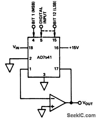
Two_quadrant_multiplier_using_a_Datel_DAC_IC10BC_D_A_convener
Published:2009/7/21 2:57:00 Author:Jessie
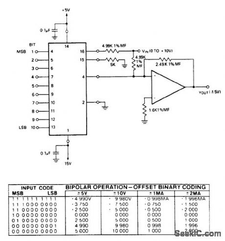
Two-quadrant multiplier using a Datel DAC-IC10BC D/A convener. The DAC-IC10BC chip is a 16-pin DIP. VIN is unipolar and the digital input is bipolar with offset binary coding. VOUT varies over the bipolar range of ±5 volts. It is recommended that full scale IREF be set to 2.0 mA; the output is then monotonic as the reference current varies over 0.5 mA to 2.0 mA (courtesy Datel Systems, Inc.). (View)
View full Circuit Diagram | Comments | Reading(1971)
Power_generation_circuit_using_n_AD7523_8_bit_multiplying_D_A_conveners
Published:2009/7/21 1:28:00 Author:Jessie

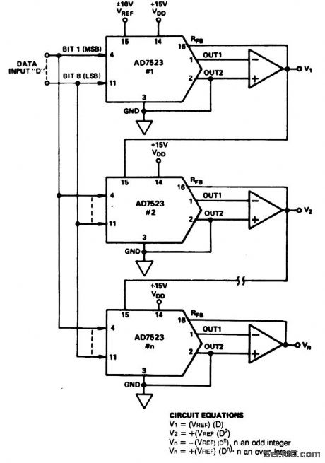
Power generation circuit using n AD7523 8-bit multiplying D/A conveners (courtesy Analog Devices, Inc.). (View)
View full Circuit Diagram | Comments | Reading(952)
Multiplier_circuit_using_an_AD534_multiplier_divider_chip
Published:2009/7/21 4:42:00 Author:Jessie
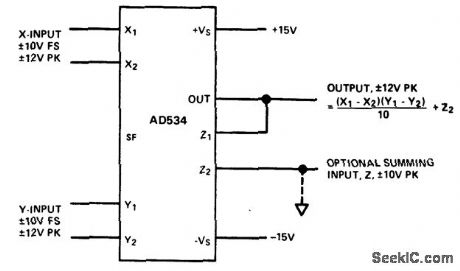
Multiplier circuit using an AD534 multiplier/divider chip (courtesy Analog Devices, Inc.). (View)
View full Circuit Diagram | Comments | Reading(1157)
Souarer_circuit_using_an_AD532_mutttpter_divider
Published:2009/7/21 4:40:00 Author:Jessie
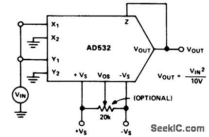
Souarer circuit using an AD532 mutttpter/divider. This chip is available as a 10-pin TO-100 or a 14-pin DIP (courtesy Analog Devices, Inc.). (View)
View full Circuit Diagram | Comments | Reading(793)
A_D_divider
Published:2009/7/21 4:39:00 Author:Jessie
A/D divider (courtesy Analog Devices, Inc.). (View)
View full Circuit Diagram | Comments | Reading(872)
D_C_D_C_CONVERTER_USES_10_KC_MVBR
Published:2009/7/21 4:38:00 Author:Jessie
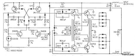
Free-running mvbr and square-hysteresis-loop transformer together fire Q1 and Q2 alternately to give constant frequency independent of changes in input voltage, while varying pulse width to give voltage regulation. Short-circuits cannot damage power supply. -E. Josephson, Satellite Power Supply has Variable Pulse Width, Electronics, 35:8, p 47-49. (View)
View full Circuit Diagram | Comments | Reading(873)
TWO_SIMPLE_TEMPERATURE_TO_TIME_CONVERTERS
Published:2009/7/7 23:55:00 Author:May
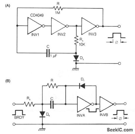


Both of these converters use CM0S inverters. Figure 105-1A shows a free-running circuit having both the pulse duration and pulse pause dependent on temperature of the diode DS. It can be used where a synchronization between the converter and something else is not required.
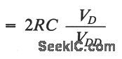
Figure 105-1B shows a one shot circuit that produces a pulse with its duration dependent of temperature of diode DS. The additional diode Df should have inverse current low enough to not influence the discharging process in the network rc when the INVA output is low. A silicon component or a GaAsP LED can be used.The converter is intended for a digital system producing a RADY pulse which disappears after the conversion process is ended. The pulse duration is approximately:where VD is the sensor diode forward voltage and VDD is the supply voltage of the CM0S chip.Resistance R must be much higher than RS A 0.1-μF capacitor can be applied in parallel with DS, if necessary, to repulse stray pickup and noise in a long cable. The circuits described can be used with a temperature sensitive resistor instead of the diode DS. (View)
View full Circuit Diagram | Comments | Reading(997)
FOUR_QUADRANT_MULTIPLYING_DAC
Published:2009/7/7 22:41:00 Author:May
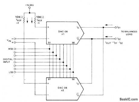
Combination of two Precision Monolithics DAC-08 D/A conveners accepts differential input voltage and produces differential current output, 0ut-put opamp is not normally required. Output analog polarity is controlled by analog input ref-erence or by offset-binary digital input word. Common-mode current present at output must be accommodated by balanced load. Differential input range is 10 V.-J. Schoeff and D. Soderquist, Differential and Multiplying Digital to Analog Converter Applications, Precision Monolithics, Santa Clara, CA, 1976, AN-19, p 3. (View)
View full Circuit Diagram | Comments | Reading(1247)
PULSE_TRAIN_TO_SINUSOID_CONVERTER
Published:2009/7/7 5:47:00 Author:May
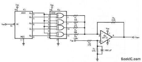
The circuit lets you convert a serial pulse stream or sinusoidal input to a sinusoidal output at 1/32 the frequency. By varying the frequency of VIN, you can achieve an output range of 107:1-from about 100 kHz to less than 0.01 Hz. The output resembles that of a 5-bit d/a converter operating on parallel digital data.
Counter IC1 generates binary codes that repeatedly scan the range from 00000 to 11111. The output amplifier adds the corresponding XOR gate outputs, VDD or ground, weighted by the values of input resistors R1 through R4. The 16 counter codes 00000 to 01111, for instance, pass unchanged to the XOR gate outputs, and cause VOUT to step through the half-sinusoidal cycle for maximum amplitude to minimum amplitude.
Counter output Q4 becomes high for the next 16 codes, causing the XOR gates to invert the Q0 through Q3 outputs. As a result, VOUT steps through the remaining half cycle from minimum to maximum amplitude. The counter then rolls over and initiates the next cycle. You can change the RI through R4 values to obtain other VOUT waveforms. VDD should be at least 12 V to assure maximum-frequency operation from IC1 to IC2.
(View)
View full Circuit Diagram | Comments | Reading(997)
REGULATED_DC_DC_CONVERTER
Published:2009/7/7 5:44:00 Author:May
View full Circuit Diagram | Comments | Reading(1063)
ZERO_IB_ERROR_V_I_CONVERTER
Published:2009/7/7 5:34:00 Author:May
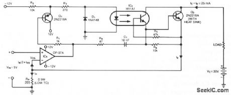
Single programming resistor RP provides an output-current range of about six decades. Note that this resistor's TC is also a potential source of error; it dissipates 125 mW when VIN= 5 V. The maximum deviation is typically 50 nA or 0.0002% of full scale. This voltage-controlled current source uses optocou-pler IC2 to eliminate an error found in more conventional circuits and which is caused by the output transistor's base current. (View)
View full Circuit Diagram | Comments | Reading(928)
PIN_PHOTODIODE_TO_FREQUENCY_CONVERTER
Published:2009/7/7 5:32:00 Author:May
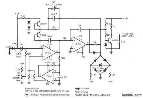
View full Circuit Diagram | Comments | Reading(891)
STEP_UP_DOWN_DC_DC_CONVERTER
Published:2009/7/7 5:27:00 Author:May
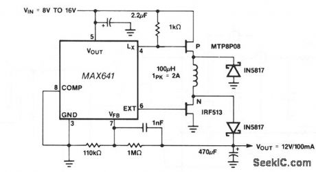
Positive output step-up and step-down dc-dc converters have a common limitation in that neither can handle input voltages that are both greater than or less than the output. For example, when converting a 12-V sealed lead/acid battery to a regulated + 12 V output, the battery voltage might vary from a high of 15 V down to 10V.
By using a MAX641 to drive separate P- and N-channel MOSFETs, both ends of the inductor are switched to allow noninverting buck/boost operation. A second advantage of the circuit over most boostonly designs is that the output goes to 0 V when shutdown is activated. Inefficiency is a drawback because two MOSFETs and two diodes increase the losses in the charge and discharge path of the inductor. The circuit delivers + 12 V at 100 mA at 70 percent efficiency with an 8-V input. (View)
View full Circuit Diagram | Comments | Reading(0)
PULSE_WIDTH_TO_VOLTAGE_CONVERTER
Published:2009/7/7 5:25:00 Author:May
View full Circuit Diagram | Comments | Reading(1409)
50_MHz_THERMAL_RMS_TO_DC_CONVERTER
Published:2009/7/7 5:23:00 Author:May
View full Circuit Diagram | Comments | Reading(1069)
VOLTAGE_RATIO_TO_FREQUENCY_CONVERTER
Published:2009/7/7 5:21:00 Author:May
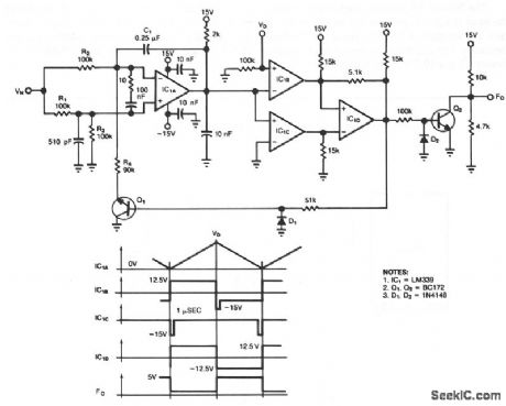
The circuit accents two positive-voltage inputs VN and VD and provides a TTL-compatible output pulse train whose repetition rate is Proportional to the ratio VN/VD. Full-scale output frequency is about 100 Hz,and linearity error is below 0.5 percent.The output F0 equals KVN/VD,where K=1/(4R2C1)provided R1=R3. Op amp ICIA alternately integrates VN/2 and - VN/2, producing a sawtooth cutou, that ramps between the VD level and ground.When transistor Q1 is on,for example, ICIA integrates -VN/2 until its Output equals VD. At that time, the IC1B comparator switches low, causing IClD's bistable output to go low, which turns off Q1. IClA's output then ramps in the negative direction. When the output reaches 0 V,the IC1C comparator switches,Q1 turns on,and the cycle repeats.Transistor Q2 converts the IC1D output to TTL-compatibl, output logic levels. Setting VD to 1.00 V yields a reciprocal voltage-to-frequency converter(Fo=KVN),and setting VN to 1.00 V yields a reciprocal voltage-to-frequency converter(Fo=KVD).
(View)
View full Circuit Diagram | Comments | Reading(974)
| Pages:11/24 1234567891011121314151617181920Under 20 |
Circuit Categories
power supply circuit
Amplifier Circuit
Basic Circuit
LED and Light Circuit
Sensor Circuit
Signal Processing
Electrical Equipment Circuit
Control Circuit
Remote Control Circuit
A/D-D/A Converter Circuit
Audio Circuit
Measuring and Test Circuit
Communication Circuit
Computer-Related Circuit
555 Circuit
Automotive Circuit
Repairing Circuit