
A/D-D/A Converter Circuit
Index 15
SELF_OSCILLATING_FLYBACK_CONVERTER
Published:2009/7/1 1:56:00 Author:May
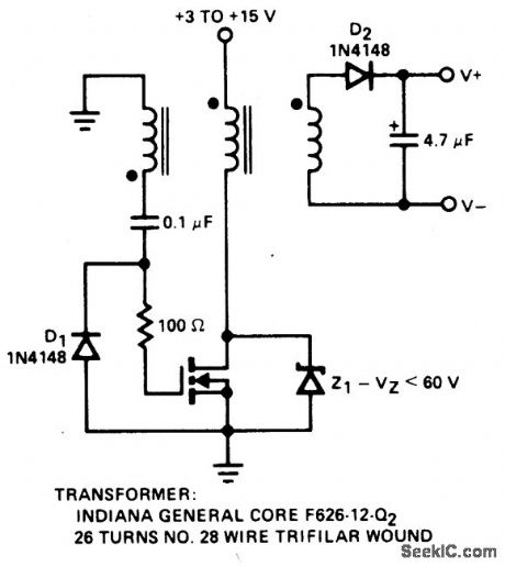
Low-power converter uses the core characteristics to determine frequency. With the transformer shown, operating frequency is 250 kHz. Diode D1prevents negative spikes from occurring at the MOSFET gate, the 100 ohm resistor is a parasitic suppressor, and Z1 serves as a dissipative voltage regulator for the output and also cUps the drain voltage to a level below the rated power FET breakdown voltage. (View)
View full Circuit Diagram | Comments | Reading(0)
PHOTODIODE_CURRENT_TO_VOLTAGE_CONVERTER
Published:2009/7/1 1:53:00 Author:May
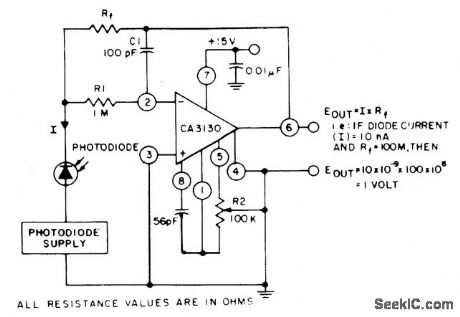
The circuit uses three CA3130 BiMOS op amps in an application sensitive to sub-picoampere input currents. The circuit provides a ground-referenced output voltage proportional to input current flowing through the photodiode. (View)
View full Circuit Diagram | Comments | Reading(1541)
PRECISION_PEAK_TO_PEAK_AC_DC_CONVERTER
Published:2009/7/1 1:48:00 Author:May
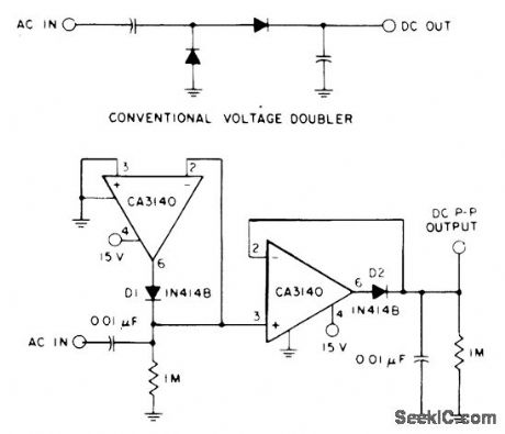
Using a CA3140 BiMOS op amp and a single positive supply converts a conventional voltage doubler with two precision diodes into a precision peak-to-peak ac-to-dc voltage converter having wide dynamic range and wide bandwidth. (View)
View full Circuit Diagram | Comments | Reading(2366)
TRIANGLE_TO_SINE_CONVERTERS
Published:2009/7/1 0:01:00 Author:May
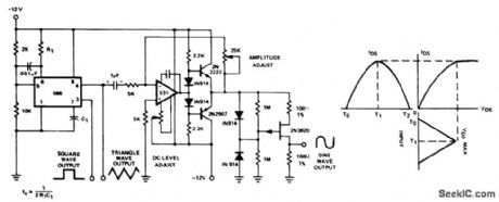
Conversion of triangle wave shapes to sinusoids is usually accomplished by diode-resistor shaping networks, which accurately reconstruct the sine wave segment by segment. Two simpler and less costly methods may be used to shape the triangle waveform of the 566 into a sinusoid with less than 2% distortion. The non-linear IDSVDS transfer characteristic of a P-channel junction FET is used to shape the triangle waveform.The amplitude of the triangle waveform is critical and must be carefully adjusted to achieve a low distortion sinusoidal output. Naturally, where additional waveform accuracy is needed, the diode-resistor shaping scheme can be applied to the 566 with excellent results since it has very good output amplitude stability when operated from a regulated supply. (View)
View full Circuit Diagram | Comments | Reading(2891)
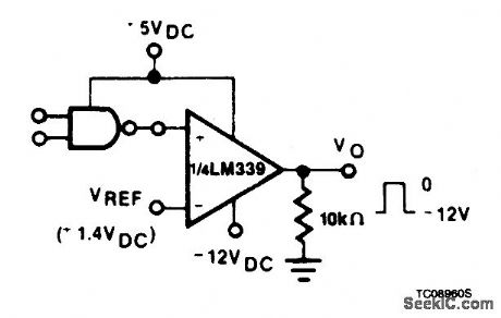
CURRENT_TO_VOLTAGE_CONVERTER_WITH_GROUNDED_BIAS_AND_SENSOR
Published:2009/6/30 23:58:00 Author:May
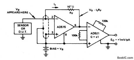
View full Circuit Diagram | Comments | Reading(1832)
CAPACITANCE_TO_PULSE_WIDTH_CONVERTER
Published:2009/6/30 23:57:00 Author:May
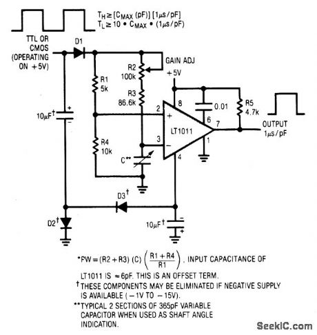
View full Circuit Diagram | Comments | Reading(884)
A_REGULATED_DC_TO_DC_CONVERTER
Published:2009/6/30 23:55:00 Author:May
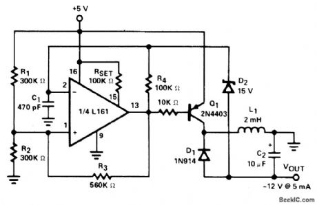
View full Circuit Diagram | Comments | Reading(939)
TTL_SQUARE_WAVE_TO_TRIANGLE_CONVERTER
Published:2009/6/30 23:53:00 Author:May
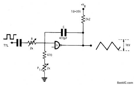
This fixed frequency triangular waveform generator driven by a TTL square wave generates typically 16-V p-p triangles at frequencies up to several MHz. It uses only one NAND open collector gate, or one open collector inverter as a fast integrator with gain.Careful successive adjustments of R and P1 are needed. When correct adjustments are reached, output amplitude and linearity are largely independent of the value of VB, from a minimum of 18 V up to 35 V. The value of C shown is for 100 kHz; at higher frequencies, it must be reduced in proportion. (View)
View full Circuit Diagram | Comments | Reading(2573)
TTL_TO_MOS_LOGIC_CONVERTER
Published:2009/6/30 23:51:00 Author:May
View full Circuit Diagram | Comments | Reading(0)
VOLTAGE_TO_CURRENT_CONVERTERS
Published:2009/6/30 23:47:00 Author:May
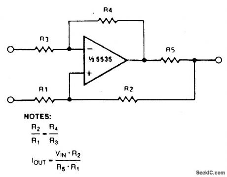
A simple voltage-to-current converter is shown in the figure. The current out is IOUT or VIN/R. For negative currents, a pnp can be used and, for better accuracy, a Darlington pair can be substituted for the transistor. With careful design, this circuit can be used to control currents of many amps. Unity gain compen-sation is necessary. (View)
View full Circuit Diagram | Comments | Reading(5364)
VOLTAGE_TO_PULSE_DURATION_CONVERTER
Published:2009/6/30 23:44:00 Author:May
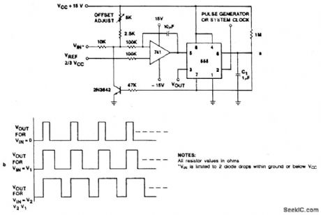
Voltage levels can be converted to pulse durations by combining an op amp and a timer IC. Accuracies to better than1% can be obtained with this circuit (a), and the output signals (b) still retain the original frequency, independent of the input voltage. (View)
View full Circuit Diagram | Comments | Reading(1027)
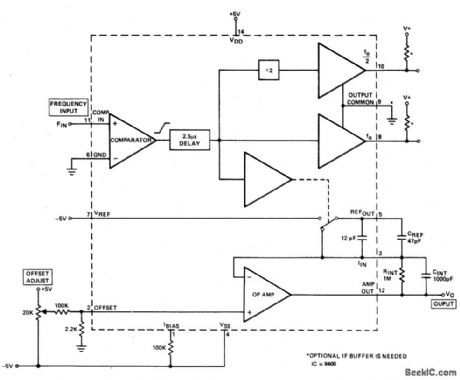
-10_V_GIVES_10_kHz
Published:2009/6/30 21:31:00 Author:May
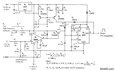
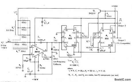
Control voltage input in range of 0 to -10 V is converted linearly to frequency of digital output pulse train haiving fullscale value of 10 kHz. Internal regulation of circuit makes operation essentially independent of ±15 V supply level.A1 is opamp integrator, A2 is comparator, and A3 is precision mono MVBR. Transistor switch Q1 connects Rb to 3.15-V reference voltage during t1 timing period of A3.—W.G.Jung, IC Timer Cookbook, Howard W.Sams, Indianapolis, IN, 1977, p184-192 (View)
View full Circuit Diagram | Comments | Reading(1451)
SINGLE_SLOPE_V_F_CONVERSlON
Published:2009/6/30 21:14:00 Author:May
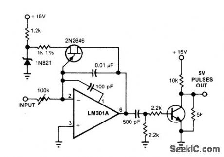
UJT forms reference that determines reset point of LM301A integrator for converting analog input voltage to proportional frequency. Output of in-tegrator ramps negative until UJT switches and drives output positive at high slew rate. Positive edge of integ rator output is differentiated by RC network and level-shifted by NPN bipolar transistor to provide logic-compatible pulse.—J. Williams, Low-Cost, Linear A/D Conversion Uses Single-Slope Techniques, EDN Magazine, Aug. 5, 1978, p 101-104. (View)
View full Circuit Diagram | Comments | Reading(1408)
20_kHz_SQUARE_WAVE_TO_DC
Published:2009/6/30 21:13:00 Author:May
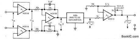
Provides accuracy within 0.1% for square-wave inputs of 3 to 7 VRMS in frequency range of 5 to 20 kHz when duty cycle is 50%. Opamps A1 and A2 are connected as differential input voltage-followers to provide high input impedance,A3 convolts to single-ended output as required by Model 440 convelter IC.A4 provides adjustable gain than roughly offsets attenuation of A3, with 2K pot being adiusted to provide desired ratio of DC output voltage to RMS value of input.—J. Renken, Differential High-Z RMS-DC Converter Has 0.1% Accuracy, EDN Magazine, May 5, 1977, p 114 and 116. (View)
View full Circuit Diagram | Comments | Reading(929)
001-10_V_to_110_OR_100_kHz
Published:2009/6/30 21:12:00 Author:May
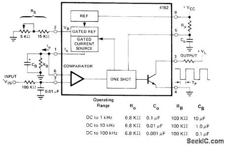
Simple voltage-to-frequency converter uses Raytheon 4152 operating from single 15-V supply to convert analog input voltage to proportional frequency of square-wave output. Maximum output frequency depends on values used for resistors and capacitors, as given in table. Suitable for applications where input dynamic range is limited and does not go to zero.— Linear Integrated Circuit Data Book, Raytheon Semiconductor Division, Mountain View, CA, 1978, p 7-45-7-46. (View)
View full Circuit Diagram | Comments | Reading(921)
CURRENT_TO_VOLTAGE
Published:2009/6/30 21:12:00 Author:May
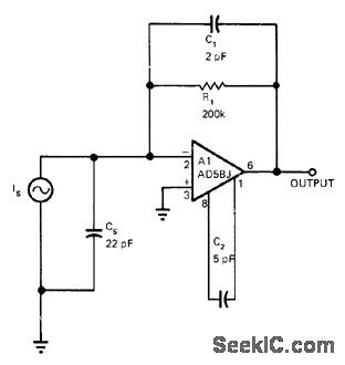
Developed for use with current-output transducers such as silicon photocells. For widest frequency response, circuit values may need some adjusting for source current and capacitance. C1, across feedback resistor of opamp, eliminates ringing around 500 kHz. If input coupling capacitor is added to reduce DC gain, circuit can be used with inductive source such as magnetic tape head.—R. S. Burwen, Current-to-Voltage Converter for Transducer Use, EDN Magazine, Dec. 15, 1972, p 40. (View)
View full Circuit Diagram | Comments | Reading(1095)
VOLTAGE_TO_FREOUENCY_GO_NO_GO
Published:2009/6/30 21:04:00 Author:May
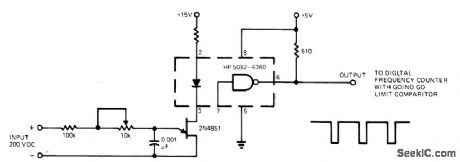
Single UJT is used as V/F converter to provide completely isolated inputs and outputs for high-voltage go/no-go test monitor When voltage exceeds predetermined limit, output to digital frequency counter exceeds corresponding frequency limit. Output can be fed directly into digital frequency-limit detector that provides go/no-go indication.—T.H.Li,VFC Used in lsolated GO-NO GO Voltage Monitor,EDN Magazine, July 5,1974, p 75. (View)
View full Circuit Diagram | Comments | Reading(1200)
HIGH_PRECISION_V_F_CONVERTER
Published:2009/6/30 21:01:00 Author:May
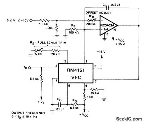
Active integrator using one section of RC3403A quad opamp improves linearhy, frequency offset, and response time of Raytheon RM4151 converter operating from single supply,Opamp develops null voltage,— Linear Integrated Circuit Data Book, Raytheon Semiconductor Division, Mountain View, CA, 1978, p 7-38. (View)
View full Circuit Diagram | Comments | Reading(1069)
DC_10_kHz_FREQUENCY_VOLTAGE_CONVERTER
Published:2009/6/30 5:54:00 Author:May
Circuit Notes
The converter generates an output vol-tage which is linearly proportional to the input frequency waveform. Each zero crossing at the comparator's input causes a precise amount of change to be dispensed into the op amp's sum-ming junction. This charge in turn flows through the feedback resistor generating voltage pulses at the output of the op amp.Capacitor (CINT) across Rtxt averages these pulses into a dc voltage which is linearly proportional to the input frequency. (View)
View full Circuit Diagram | Comments | Reading(1124)
A_D_converter_for_3_digit_LED_display
Published:2009/7/24 10:01:00 Author:Jessie
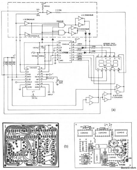
This circuit shows a CA3162A connected to a CD4511B decoder/driver to operate a common-cathode LED display. Figure 6-21B shows the PC tenmplate and component layout. The additional logic shown within the dotted area allows the display of negative numbers as low (as -99 mV), depending on the Position of the DP1/DP2 switch. The sampling rate can be changed from 4 to 96 Hz when pin 6 of'the CA3162A is connected to +5 V. To adjust, follow the proccdure described for Fig. 6-20. Harris Semiconductors, Data Acquisition, 1991, p. 2-6, 2-7. (View)
View full Circuit Diagram | Comments | Reading(2121)
| Pages:15/24 1234567891011121314151617181920Under 20 |
Circuit Categories
power supply circuit
Amplifier Circuit
Basic Circuit
LED and Light Circuit
Sensor Circuit
Signal Processing
Electrical Equipment Circuit
Control Circuit
Remote Control Circuit
A/D-D/A Converter Circuit
Audio Circuit
Measuring and Test Circuit
Communication Circuit
Computer-Related Circuit
555 Circuit
Automotive Circuit
Repairing Circuit