
A/D-D/A Converter Circuit
Index 19
FAST_VOLTAGE_OUTPUT_D_A_CONVERTER
Published:2009/6/26 2:11:00 Author:May
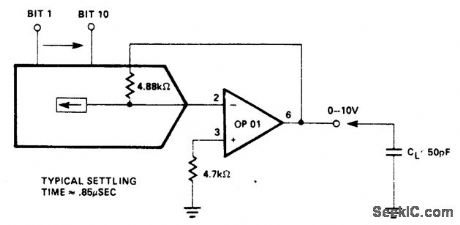
View full Circuit Diagram | Comments | Reading(797)
10_BIT_D_A_CONVERTER
Published:2009/6/26 2:10:00 Author:May
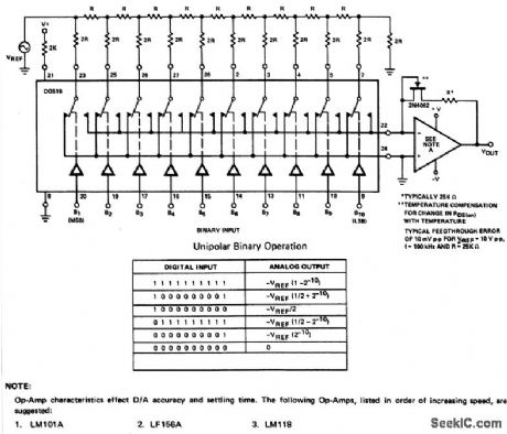
0p-Amp characteisties effect D/A accuracy and setding time. The following Op-Amps, listed in order of increasing speed, are suggested:1.LM101A 2.LF156A 3.LM118 (View)
View full Circuit Diagram | Comments | Reading(978)
14_BIT_BINARY_D_A_CONVERTERUNIPOLAR
Published:2009/6/26 2:02:00 Author:May
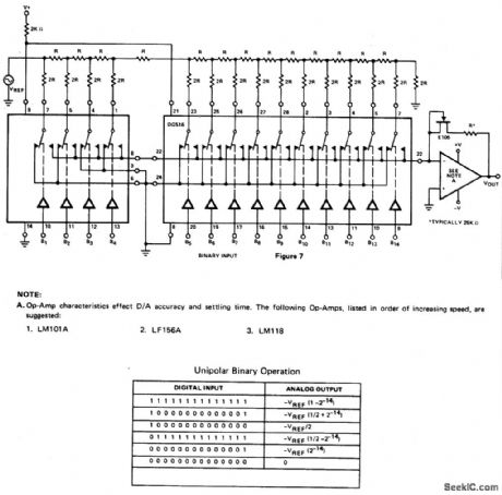
View full Circuit Diagram | Comments | Reading(780)
400_V,60_W_PUSH_PULL_DC_DC_CONVERTER
Published:2009/6/25 4:40:00 Author:May
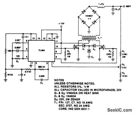
Circuit Notes
The TL494 switching regulator governs the operating frequency and regulates output voltage, Switching frequency approximately 100 kHz for the values shown。Output regulation IS typically 1.25% from no-load to full 60 W。 (View)
View full Circuit Diagram | Comments | Reading(5102)
REGULATED_DC_TO_DC_CONVERTER
Published:2009/6/25 4:38:00 Author:May
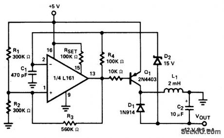
Circuit Notes
Low power dc to dc converter obtained by adding a flyback circuit to a square wave oscil-lator. Operating frequency is 20 kHz to minimize the size of L1 and C2. Regulation is achieved by zener diode D2. Maximum current available before the convener drops out of reg-ulation is 5.5 rnA. (View)
View full Circuit Diagram | Comments | Reading(902)
SELF_OSCILLATING_FLYBACK_CONVERTER
Published:2009/6/25 2:43:00 Author:May
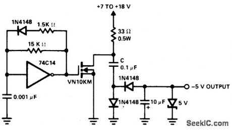
A low-power converter suitable for deriving a higher voltage from a main system rail in an on-board application. With the transformer shown, the operating frequency is 250kHz. Z1 serves as a dissipative voltage regulator for the output and also clips the drain voltage to a level below the rated VMOS breakdon boltage. (View)
View full Circuit Diagram | Comments | Reading(1876)
BCD_TO_ANALOG_CONVERTER
Published:2009/6/25 2:05:00 Author:May
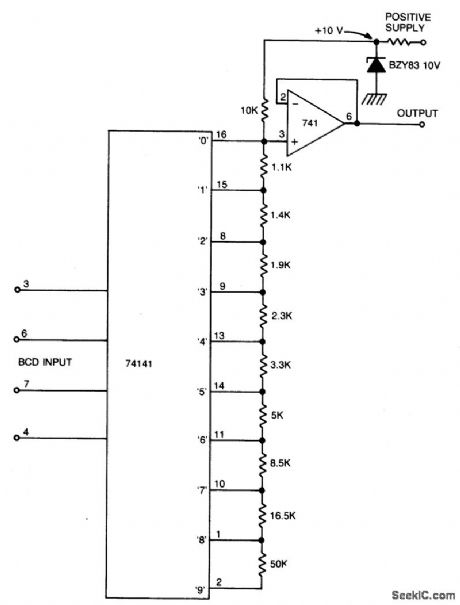
This circuit will convert four-bit BCD into a variable voltage from 0-9 V in 1 V steps. The SN74141 is a Nixie driver, and has ten open-collector outputs. These are used to ground a selected point in the divider chain determined by the BCD code at the input, and so produce a corresponding voltage at the output. Accuracy of the circuit depends on the tolerance of the resistors and the accuracy of the reference vol-tage. However, presets can be used in the di-viderchain, with correct calibration. The 741 is used as a buffer. (View)
View full Circuit Diagram | Comments | Reading(1995)
TTL_TO_MOS_LOGIC_CONVERTER
Published:2009/6/25 2:39:00 Author:May
View full Circuit Diagram | Comments | Reading(0)
SINE_WAVE_TO_SQUARE_WAVE_CONVERTER
Published:2009/6/25 2:38:00 Author:May
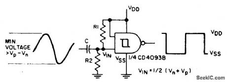
The sine input is ac coupled by capacitor C; R1 and R2 bias the input midway between Vn and Vp, the input threshold voltages, to provide a square wave at the output. (View)
View full Circuit Diagram | Comments | Reading(0)
FAST_LOGARITHMIC_CONVERTER
Published:2009/6/25 2:36:00 Author:May

View full Circuit Diagram | Comments | Reading(915)
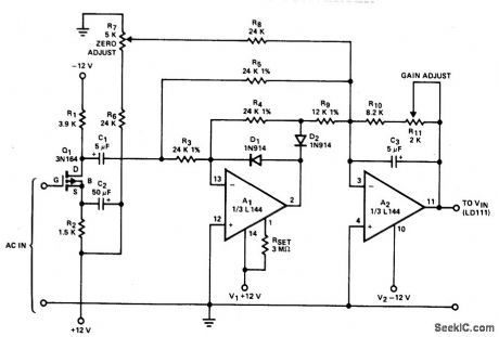
MULTIPLEXER_BCE_TOTPARALLEL_BCD_CONVERTER
Published:2009/6/25 2:35:00 Author:Jessie
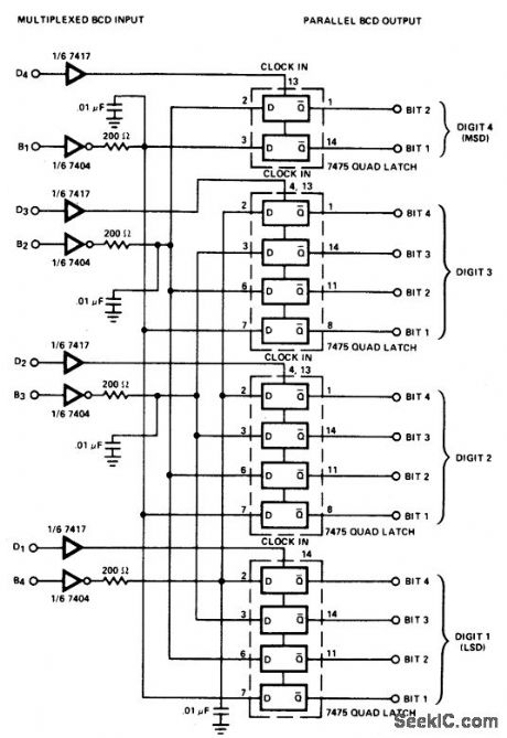
Converter consists of four quad bistable latches activated in the proper squence by the digit srtobe output of the LD110. The complemented outputs (Q) of the quad latch set reflects the state of the bit outputs when the digit strobe goes high. It will maintain this state when the digit srobe goes low. (View)
View full Circuit Diagram | Comments | Reading(920)
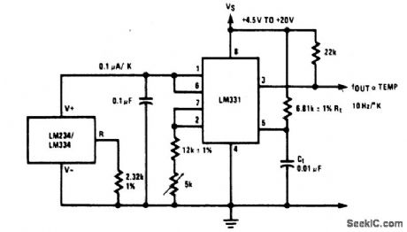
TEMPERATURE_TO_FREQUENCY_CONVERTER
Published:2009/6/25 2:30:00 Author:Jessie
View full Circuit Diagram | Comments | Reading(0)
WIDEBAND_HIGH_CREST_FACTOR_RMS_TO_DE_COMVERTER
Published:2009/6/25 2:26:00 Author:May
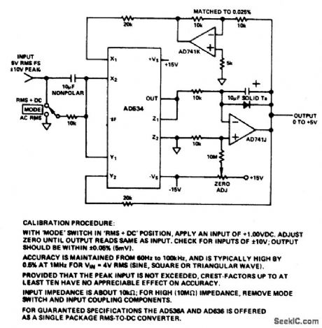
View full Circuit Diagram | Comments | Reading(0)
OHMS_TO_VOLTS_CONVERTER
Published:2009/6/25 2:29:00 Author:Jessie
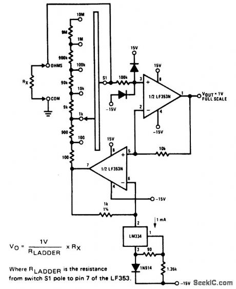
View full Circuit Diagram | Comments | Reading(1107)
LIGHT_INTENSITY_TO_FREQUENCY_CONVERTER
Published:2009/6/25 2:28:00 Author:Jessie
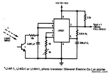
View full Circuit Diagram | Comments | Reading(1561)
VOLTAGE_TO_CURRENT_CONVERTER
Published:2009/6/25 2:24:00 Author:May
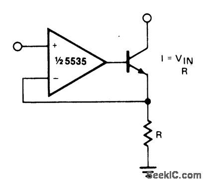
The current out is IOUT≌VIN/R. For negative currents, a PNP can be used and, for better accuracy, a Darlington pair can be substituted for the transistor. With careful design, this cir-cuit can be used to control currents of many amps. Unity gain compensation is necessary. (View)
View full Circuit Diagram | Comments | Reading(0)
POLARITY_CONVERTER
Published:2009/6/25 2:22:00 Author:May
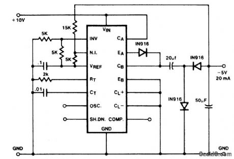
The capacitor-diode output circuit is used here as a polarity converter to generate a -5 volt supply from +15 volts. This circuit is use-ful for an output current of up to 20 mA with no additional boost transistors required. Since the output transistors are current limited, no addi-tional protection is necessary. Also, the lack of an inductor allows the circuit to be stabilized with only the output capacitor. (View)
View full Circuit Diagram | Comments | Reading(1077)
CURRENT_TO_VOLTAGE_CONVERTER_WITH_1_Accuracy
Published:2009/6/25 2:21:00 Author:May
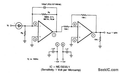
A filter removes the dc component of the rectified ac, which is then scaled to RMS. The output is linear from 40 Hz to 10 kHz or higher. (View)
View full Circuit Diagram | Comments | Reading(921)
AC_TO_DC_CONVERTER
Published:2009/6/25 2:20:00 Author:May
This circuit includes a PMOS enhancement-mode FET input buffer amplifier, coupled to a classical absolute value circuit which essentially eliminates the effect of the forward voltage drop across diodes D1 and D2. (View)
View full Circuit Diagram | Comments | Reading(1959)
WIDE_RANGE_CURRENT_TO_FREQUENCY_CONVERTER
Published:2009/6/25 2:19:00 Author:May
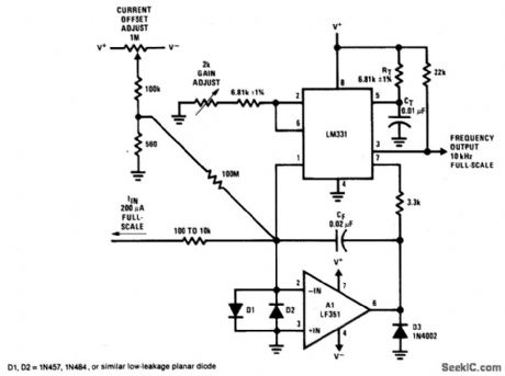
View full Circuit Diagram | Comments | Reading(987)
| Pages:19/24 1234567891011121314151617181920Under 20 |
Circuit Categories
power supply circuit
Amplifier Circuit
Basic Circuit
LED and Light Circuit
Sensor Circuit
Signal Processing
Electrical Equipment Circuit
Control Circuit
Remote Control Circuit
A/D-D/A Converter Circuit
Audio Circuit
Measuring and Test Circuit
Communication Circuit
Computer-Related Circuit
555 Circuit
Automotive Circuit
Repairing Circuit