
A/D-D/A Converter Circuit
Index 16
Interfacing_D_A_converters_with_digital_logic_families
Published:2009/7/24 9:54:00 Author:Jessie
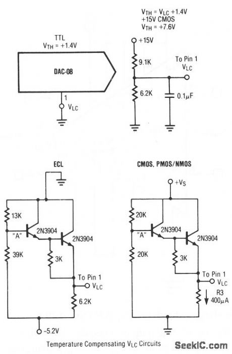
This circuit shows the interface circuits that are required to interface a typical TTL DAC with ECL,CMOS, PMOS, and NMOS digital devices. Raytheon Linear Integrated Circuits, 1989, p. 6-15. (View)
View full Circuit Diagram | Comments | Reading(946)
01_Hz_100_kHz_V_F
Published:2009/6/30 3:35:00 Author:May
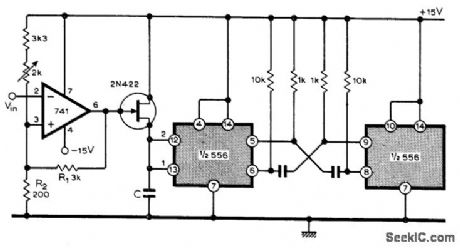
Uses NE556 timer in dual mode in combination with opamp and FET for linear voltage-to-frequency conversion with output rangefrom 0.1 Hz to 100 kHz. Operatbg frequency is 0.91/2RC where R is resistance of FET.—K. Kraus, Linear V-F Converter, Wireless World, May 1977, p 80. (View)
View full Circuit Diagram | Comments | Reading(2079)
V_F_CONVERTER_WITH_005_LINEARITY
Published:2009/6/30 3:34:00 Author:May
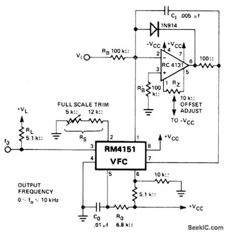
Raytheon RM4151 converter is used with integrator opamp to give highly linear conversion of inputs up to -10 VDC to proportional frequency of square-wave output. With maximum input of -10 V, adjust 5K full-scale trimpot for maximum output frequency of 10 kHz. Set offset adjust pot to give 10-Hz output for input of -10 mV. To operate from single positive supply, change opamp to RC3403A.— Linear Integrated Circuit Data Book, Raytheon Semiconductor Division, Mountain View, CA, 1978, p 7-38. (View)
View full Circuit Diagram | Comments | Reading(1083)
10_Hz_TO_10_kHz_V_F
Published:2009/6/30 3:29:00 Author:May
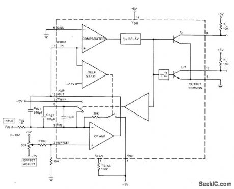
External circuit shown for Teledyne 9400 Voltage-to-frequency converter provides means for trimming zero location and full-scale frequency value of output For 10-kHz full-scale value, set Vin to 10 mV and trim with 50K offset adjust pot to get 10-Hz output, then set V1, to 10.000 V and trim either Rin, VREF, or CREF to obtain 10-kHz output.—M. 0. Paiva, Applications of the 9400 Voltage to Frequency Frequency to Voltage Converter, Teledyne Semiconductor, Mountain View, CA, 1978, AN-10, p 3-5. (View)
View full Circuit Diagram | Comments | Reading(1370)
FOUR_OUADRANT_ALGEBRAIC
Published:2009/6/30 3:21:00 Author:May

Two Precision Monolithics DAC-08 D/A converters perform fast algebraic summation of two digital input words and feed OP-02 opamp that provides direct analog output which is algebraic sum of words A and B in all four quadrants.—J. Schoeff and D. Soderquist, Differential and Multiplying Digital to Analog Converter Applications, Precision Monolithics, Santa Clara, CA, 1976, AN-19, p 7. (View)
View full Circuit Diagram | Comments | Reading(1580)
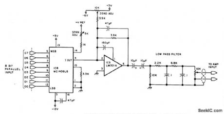
CURRENT_CONVERTER
Published:2009/6/30 3:14:00 Author:May

Converts 8-bit TTL digital inputs to process current in range of 4 to 20mA, for microprocessor control of industrial operations. Fixed 0.5-mA current is added to DAC output current varying between0 and 2.0 mA and multiplied by factor of 8 to produce final output current of 4-20 mA. To calibrate, connect ammeter between output and ground, then apply +23 V ± 7 V and -5 V ± 1 V to converter. Make digital inputs all 0s (less than +0.8 V). Adjust R1 until output current is 4.0 mA.Changedigital inputs to all is (greater than +2.0 V), and adjust R2 until output current is 20 mA.—D. Soderquist, Build Your Own 4-20 mA Digital to Analog Converter, Instruments & Control Systems, March 1977, p 57-58. (View)
View full Circuit Diagram | Comments | Reading(1183)
SIMPLE_DAC
Published:2009/6/30 3:05:00 Author:May
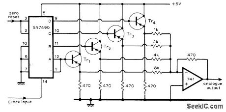
Transistors are either saturated or cut off by outputs of clock-controlled SN7490 BCD counter, Portions of emitter voltages of the four transistors are added in ratios 1:2:4:8 by 741 summing opamp to obtain analog output. Article tells how two such circuits can be combined for use in two-digit DVM.—D. James, Simple Digital to Analogue Converter, Wireless World, June 1974, p 197. (View)
View full Circuit Diagram | Comments | Reading(2385)
ANALOG_SUM_OF_DIGITAL_NUMBERS
Published:2009/6/30 3:04:00 Author:May
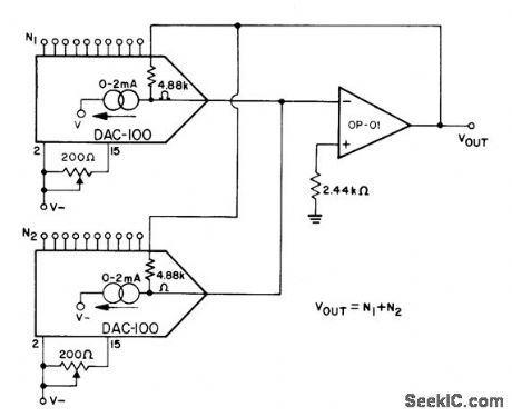
Two Precision Monolithics DAC-100 D/A convelters and op-01 opamp combine conversion with adding to give high-precision DC output voltage,200-ohm pots are adjusted initially to give exactly desired output for input of all 0s,— 8 &10 Bit Digital-to-Analog Converter, Precision Monolithics, Santa Clara, CA, 1977、DAC-100, p 5. (View)
View full Circuit Diagram | Comments | Reading(963)
DAC_FOR_SPEECH
Published:2009/6/30 3:00:00 Author:May
Audio signals stored in 8-channel digital form in computer are converted back into analog form for feed through low-pass filter to input of audio amplifier. Can be used for computer-controlled synthesis of speech from phonemes in any language or for providing voice replies to queries. Pin 7 of IC9 is +12 V, and pin 4 is -12V.—S. Ciarcia, Talk to Me! Add a Voice to Your Computer for $35, BYTE, June 1978, p 142-151 (View)
View full Circuit Diagram | Comments | Reading(1602)
_15_V_TO__27_V
Published:2009/6/30 2:47:00 Author:May
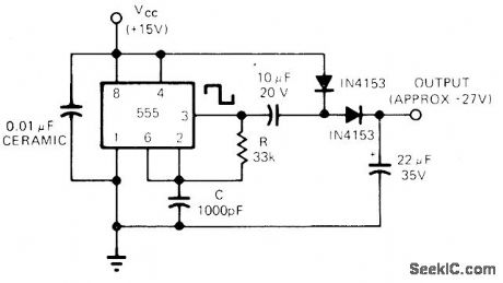
Uses 555 timer in self-triggered mode as square-wave generator operating at about 20 kHz, followed by voltage-doubling rectifier. Provides approximate doubling of voltage without use of transformer. Maximum load current is about 80 mA.—M. Strange, IC Timer Makes Transformerless Power Converter, EDN Magazine, Dec. 20, 1973, p 81. (View)
View full Circuit Diagram | Comments | Reading(2002)
±15_V_FROM_12_V
Published:2009/6/30 2:46:00 Author:May

Steps up output of 12-V bat-tery to voltages required by PLL such as NE561. Uses 900-Hz sine-wave oscillator and LM380N AF amplifier to drive voicecoil side of standard 500-ohm to 3.2-ohm output transformer having bridge rectifier across center-tapped primary. With 10-mA loads, maximum ripple is 15 mV P-P. With receiver quiet, 900-Hz hum is audible, but is normally lost under background noise. Oscillator choke (about 700 mH) is 800 turns of No. 44 magnet wire in Ferroxcube 30 pot core.—R. Megirian, Build a Noise-Free Power Supply, 73 Magazine, Dec. 1977, p 208-209. (View)
View full Circuit Diagram | Comments | Reading(1294)
_15_V_TO__12_V
Published:2009/6/30 2:44:00 Author:May
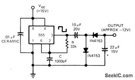
Simple transformerless power converter uses 555 timer in self-triggered mode as square-wave generator, followed by voltage-doubling rectifier. Values shown for R and C give frequency of about 20 kHz, which permits good filtering with relatively small capacitors. Maximum load current is about 80 mA.—M. Strange, IC Timer Makes Transformerless Power Converter, EDN Magazine, Dec. 20, 1973,p 81. (View)
View full Circuit Diagram | Comments | Reading(1728)
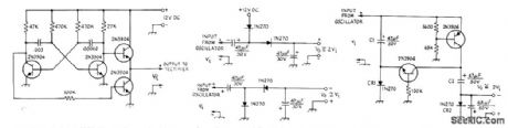
_12_V_TO_-2_V
Published:2009/6/30 2:42:00 Author:May
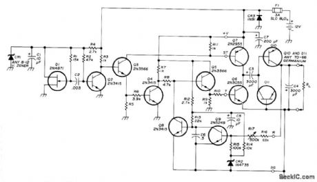
High-effkiency polarity inverter for mobile applications provides wellregulated ad justable negative output voltage at 2 A from positive auto battery source. Stable UJT oscillator al drives transistor Q2 to produce symmetrical square wave. Q3 buffers output and furnishes driving power for inverter Q4 and output stage Q7. Q4 and Q5 together drive Q6 into complete saturation. Q6 and Q7 form complementary-symmetry output operating in saturation mode, with only one transistor turned on at a time. As they are alternately switched on and off, square wave alternating between ground and nearly battery potential is applied to Q3. Q10 and Q11 are connected as diodes for clamping square wave negatively. Output voltage is regulated by transistor feedback loop Q8 and Q9, with zener CR2 providing stable reference. R10 is 100 ohms for 2 A maximum; increasing its value improves efficiency but reduces maximum current.—J. R. Laughlin, Medium Current Polarity Inverter, Ham Radio, Nov. 1973, p 26-30. (View)
View full Circuit Diagram | Comments | Reading(1746)
_12_V_TO__20_V
Published:2009/6/30 2:37:00 Author:May
Developed for use with mobile equipment when DC voltage higher than that of auto battery is needed. One application is trickle-charging 12-V nickel-cadmium batteries. Un is 555 timer operated as free-running square-wave oscillator. Frequency is determined by R1, R2, and 02; with values shown, it is about 6 kHz.C1 reduces 6-kHz signal radiated back through input lines. If converter is used with high-frequency receiver, insert 100-μH RF chokes in power leads to suppress harmonics of 6 kHz. For 12-V input, typical outputs are 20.4 V at 10 mA, 19.9 V at 20 mA, and 17.7 V at 50 mA. All diodes are 1N914, 1N4148 or equivalent.—G. A. Graham, Low-Power DC.DC Converter; Ham Radio, March 1975, p 54-56. (View)
View full Circuit Diagram | Comments | Reading(1128)
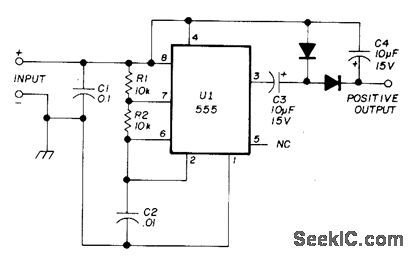
0_TO_-10_V_FROM__12_V
Published:2009/6/30 2:35:00 Author:May


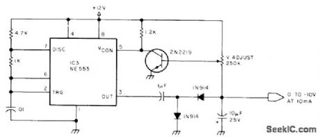
Variable-output converter using NE555 timer delivers negative output votage required by some interface devices and D/A converters used with microprocessors.—S. Ciarcia,Build a 5 W DC to DC Converter, BYTE,Oct,1978、p 22, 24, 26, 28, and 30-31. (View)
View full Circuit Diagram | Comments | Reading(1068)
REGULATED__900_V_FROM__6_V
Published:2009/6/30 2:32:00 Author:May

CA3094 programmable opamp is connected as oscillator for driving step-up transformer that develops suit. able high voltage for rectification in diode network. Sample of +900 V regulated output is fed to CA3080A variable opamp through 198-meg ohm resistor of voltage divider to control pulse repetition rate of oscillator. Magnitude of regulated output is controlled by pot R. Regulation is within 1% for loads of 5 to 26μA. DC-to-DC conversion efficiency is about 50%.— Circuit Ideas for RCA Linear ICs, RCA Solid State Division, Somerville, NJ, 1977, p 19. (View)
View full Circuit Diagram | Comments | Reading(1050)
TRANSFORMERLESS_POSITIVE_TO_NEGATIVE
Published:2009/6/30 2:30:00 Author:May
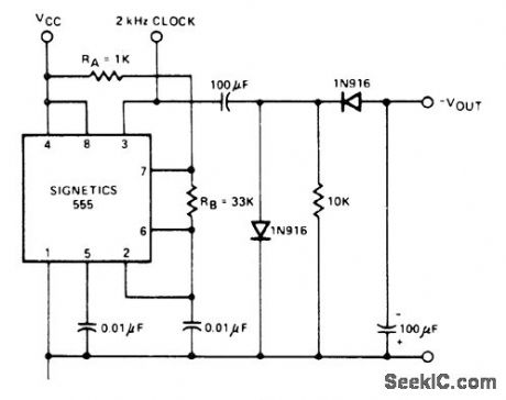
Used to derive negative supply voltage from positive supply voltage, while at same time generating 2-kHz dock signal, Negative output voltage tracks DC input voltage linearly, but magnitude is about 3 V lower. Circuit does not provide regulation.— Signetics Analog Data Manual, Signetics, Sunnyvale, CA, 1977, p 729. (View)
View full Circuit Diagram | Comments | Reading(1136)
±15_V_FROM__5_V
Published:2009/6/30 2:30:00 Author:May
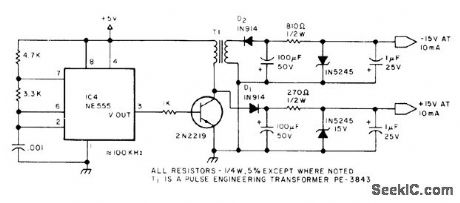
Provides positive and negative higher voltages required by some interface devices used with microprocessors. NE555 timer is connected as 100-kHz oscillator that switches transistor on and off, inducing current in primary of T1. High-voltage spike reflected back to collector of transistor by pulse transformer is routed through D1 to filter-regulator for providing positive output.—S. Ciarda, Build a 5 W DC to DC Convener, BYTE, Oct. 1978 p 22, 24,26,28, and 30-31. (View)
View full Circuit Diagram | Comments | Reading(2361)
POLARITY_REVERsER
Published:2009/6/30 2:28:00 Author:May

Simple RC osdllator operating at about 1200 Hz can be used with choice of rectifier circuits to provide negative or positive voltages equal to or higher than DC supply, without use of transformer. Output transistors connect Ioad altemately to positive supply and to ground for high operating efficiency. Two-diode voltage doubler with connection to 12-V supply gives positive output.Other diode rectifier cilcuit doubles oscillatol output and gives negative supply. Negative doubler uses switching transistors. All three rectifier circuits provide common ground from supply to output.—J. M. Pike, Negative and High Voltagesfrom a Positive Supply, QST, Jan.1974, p 23-25 (View)
View full Circuit Diagram | Comments | Reading(0)
_8_V_FROM__5_V
Published:2009/6/30 2:26:00 Author:May
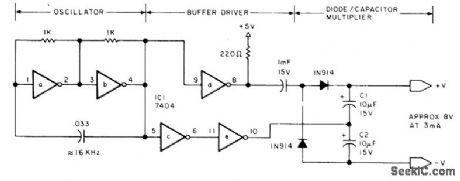
Oscillator operating atabout 16 kHz steps up 5-V supply voltage of microprocessor to 8 V for driving special interface circuits. Sections c,d,and e of 7404 hex inverter form buffer and driver for voltage-dou-bling rectifier.—S. Ciarcia,Build a 5 W DC to DC to DC converter,BYTE,Oct.1978, p22, 24, 26, 28, and 30-31. (View)
View full Circuit Diagram | Comments | Reading(1895)
| Pages:16/24 1234567891011121314151617181920Under 20 |
Circuit Categories
power supply circuit
Amplifier Circuit
Basic Circuit
LED and Light Circuit
Sensor Circuit
Signal Processing
Electrical Equipment Circuit
Control Circuit
Remote Control Circuit
A/D-D/A Converter Circuit
Audio Circuit
Measuring and Test Circuit
Communication Circuit
Computer-Related Circuit
555 Circuit
Automotive Circuit
Repairing Circuit