
A/D-D/A Converter Circuit
Index 5
MICROPOWER_STET_UP_CONVERTER
Published:2009/7/13 1:48:00 Author:May
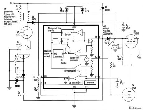
This circuit can start with inputs as low as a diode drop, i.e., 0.6 V. It provides a 5-V output with 15-mA current capability, but for this application, the load current must be limited. The circuit pow-ers a meter from the drop across a single diode in a 4- to 20-mA current loop, and provides 77 percent efficiency at a current of 0.5 mA (with diode D6 shorted). Load current available to the meter (Iload) is limited by the 4-mA minimum loop current. Transistor Q1 and transformer T1 form a resonant tank circuit that self-oscillates at a frequency of approximately 1/L1R1.R1 is a current-limiting resistor. At 50 kHz, with an input of 0.6 V, the value shown for resistor R1 (33 Ω) limits the maximum current into the base of transistor Q1 to 20 mA. The primary inductance of transformer T1, although not a crucial parameter, should be 660 μH for this value resistor of R1.
(View)
View full Circuit Diagram | Comments | Reading(1094)
±20_V_CHARGE_PUMP_BOOST_CONVERTER
Published:2009/7/13 1:41:00 Author:May
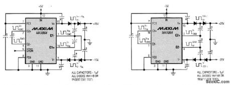
A low-power converter of 5 to ±20 V can be made surprisingly small by enhancing a dual-output charge-pump IC with an extra boost stage composed of discrete diodes. Such supplies are useful for LCD power supplies, LCD bias, and varactor tuners. The MAX864 on its own can generate ±10 V (minus load-proportional losses) from a 5-V input, or ±6.6 V from a 3.3-V input. Using additional diode-capacitor stages, these outputs can be doubled again to approximately ±4Vin or multiplied by 1.5 to approximately ±3Vin. Note that the external diode/capacitor network connects to C1 for ±15-V outputs or to C2 for ±20V outputs. (View)
View full Circuit Diagram | Comments | Reading(1211)
DC_TO_DC_CONVERTER_FOR_DIGITAL_PANEL_METERS
Published:2009/7/16 21:06:00 Author:Jessie
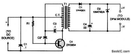
Often a digital panel meter is used in an application where the meter is on the hot side of a Circuit This supply will provide the 9-to 12-Vdc floating supply for the meter. (View)
View full Circuit Diagram | Comments | Reading(1530)
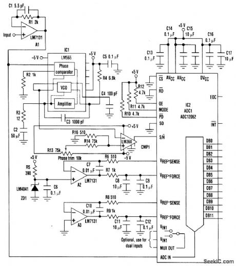
ISOLATED_3_V_TO_5_V_DAC
Published:2009/7/12 22:50:00 Author:May
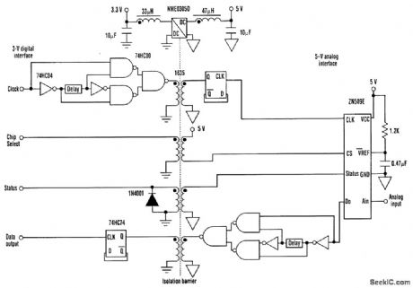


The circuit uses a low-power (1 W) dc-to-dc converter for the power isolation and a transformer isolator/translator for the data interface. The transformer isolator not only provides the galvanic iso-lation required, but also converts the data signals between 3-V and 5-V levels. As a result, no additional level conversion is required. The ADC can run at 1-MHz clock rates. To allow the 50 percent duty cycles (clock and data signals) to pass through a transformer isolator requires an edge-detection and conversion technique. The edge detector is built from simple logic gates (two inverters and three NAND gates) and a short delay (either a delay line or a passive RC circuit can be used). The signal is rebuilt with a D-type flip-flop. Using a four-channel isolator allows full control over the ADC to be exercised. Conversion is requested by pulling the Chip Select pin low, and a Status high for one clock cycle is reported back to acknowledge conversion start. The first data bit (MSB) then is presented onto the data line, and all eight bits are transferred with a further Status signal at the end of conversion. Conversion can be requested asynchronously with the system clock, if necessary, and the Status flag can be used to poll the controlling logic circuitry. Filtering is placed on either side of the dc-to-dc converter to reduce power-supply ripple and prevent noise on the logic power supply from affecting the analog system. Although not shown, all ICs have 0.22-μF decoupling capacitors. (View)
View full Circuit Diagram | Comments | Reading(1145)
TIME_TO_VOLTAGE_CONVERTER
Published:2009/7/12 22:18:00 Author:May
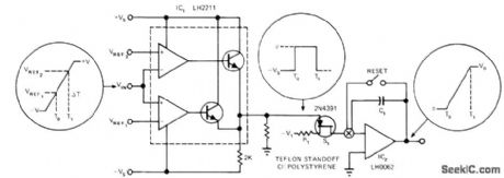
Dual comparator, solid-state switch, and fast FET opamp provide flexibility, range, and accuracy required for using converter in computer-controlled test system. IC2 operates as integrator and sample-and-hold circuit. Reference voltages of IC1, VREF1, and VFEF2 allow time measurements of signal having ehher positive or negative voltage levels or both. Floating output stdges of comparators provide voltage translation for FET switch S1. With S1 closed, IC2 integrates for time period during which input signal is below reference voltages. With S1 open, IC2 holds final voltage value. Measurement range is from 1 μs to several hours.-C. Wojslaw, Wide Range Time Measurements Simplified, EDN Magazine,-Feb.5, 1974, p 95-96.
(View)
View full Circuit Diagram | Comments | Reading(1193)
COMPUTER_CONTROLLED_A_D_CONVERTER
Published:2009/7/12 22:18:00 Author:May
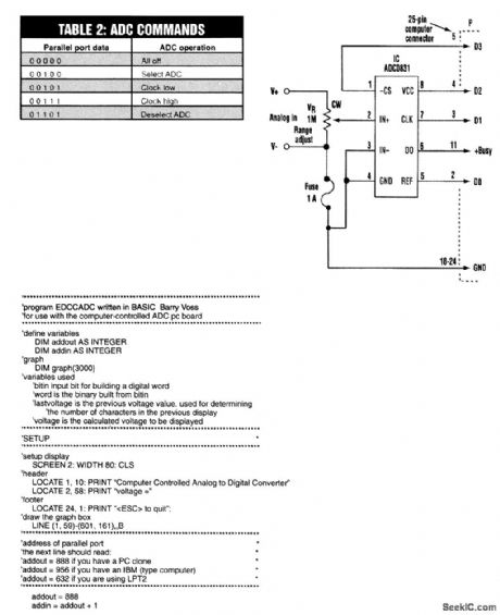
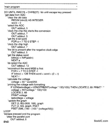
This simple, inexpensive computer-controlled A/D converter (ADC) plugs into a PC parallel port. The 8-bit peripheral device requires only seven components controlled to imponents and is imkplement and is completely controllde by a short BASIC program. (View)
View full Circuit Diagram | Comments | Reading(1150)
ASCLL_TO_BAUDOT_CONVERTER
Published:2009/7/11 3:28:00 Author:May
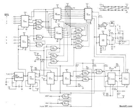
Converts parallel ASCLL output of keyboard to serial Baudot format for driving Baudot teleprinters.conversion circuit can save several hundred bytes of computer or microprocessor storage,making this memeory space available for other purposes Article gives conversion table for for all capital and lowercase alphabetic characters,numeric,and punctuation.-J.ALehman and R.Graham,ASCLL to Baudot...er...Murray(the Hard Way ),Kilobaud,June 1978,p 80-83.
(View)
View full Circuit Diagram | Comments | Reading(993)
ADC_CONVERTER_SYNCHRONOUS_DEMODULATION
Published:2009/7/17 3:52:00 Author:Jessie
Digital radio techniques promise to dramatically enhance receiver capabilities. Directly converting the IF (intermediate frequency) to a digital signal facilitates digital signal processing of demodulated signals. The example described here features an AM radio detector circuit for the typical IF of 455 kHz. For RF demodulation, the input is sampled at a rate exactly equal to the input-signal frequency. The digital output signal, which is actually an alias of the input, is the recovered modulation. (View)
View full Circuit Diagram | Comments | Reading(2363)
True_rms_converter
Published:2009/7/17 3:49:00 Author:Jessie
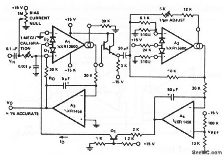
This circuit uses both sections of an XR-13600 (Fig. 11-1B). The circuit is essentially an AGC amplifier, which adjusts the gain such that the output of A1 is constant. The calibration potentiometer is set such that VO reads directly in rms volts. EXAR Corporation Databook 1990, p 5-257 (View)
View full Circuit Diagram | Comments | Reading(1189)
ac_TO_dc_CONVERTER
Published:2009/7/10 22:02:00 Author:May
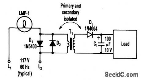
By coupling two back-to-back diodes in series with an ac power circuit, a voltage of about 1.4 Vpp can be obtained. This voltage is useful for exciting the primary coil of a small transformer. The voltage induced in the secondary coil can then be rectified and used to power solid-state control circuits. The forward-voltage drop of the diodes is inherently constant and stable over a wide range of accircuit power variations.The resulting voltage developed across the transformer windings is also free from variation that might be caused by changes in the circuit's current or voltage.
In the circuit, a lamp (LMP-1) is connected to the primary ac input line (L1 and L2) through a pair of inverse-parallel-connected power diodes (D1and D2). As power flows to the lamp, a drop of about 0.7 V is alternatively developed across each of the diodes. This voltage feeds the primary of a small ransformer (T1). T1 can be a small 8-Ω to 500-Ω transistor radio output, etc. This will deliver about 11 Vpp across its secondary winding. LMP1 can be a small 120-V lamp of 5 to 25 W, etc. (View)
View full Circuit Diagram | Comments | Reading(0)
Precision_frequency_to_voltage_converter
Published:2009/7/19 21:30:00 Author:Jessie
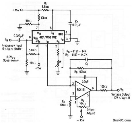
Figure 12-5 shows an FVC that is similar to Fig. 12-4, except that linearity, offset, and response time is improved by adding an op amp to form an active low-pass filter at the output. Raytheon Linear Integrated Circuits 1989 p 7-10. (View)
View full Circuit Diagram | Comments | Reading(1262)
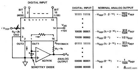
10_bit_multiplying_D_A_convener_in_bipolar_operation
Published:2009/7/20 4:26:00 Author:Jessie
10-bit multiplying D/A convener in bipolar operation. In this configuration the D/A converter is set up for four-quadrant multiplication (courtesy Analog Devices, Inc.). (View)
View full Circuit Diagram | Comments | Reading(985)
Unipolar_binary_digital_to_voltage_converter_using_an_AD7520_D_A_converter
Published:2009/7/20 3:43:00 Author:Jessie
Unipolar binary digital-to-voltage converter (two-quadrant multiplier) using an AD7520 D/A converter. R1 and R2 provide gain adjustment capability (courtesy Analog Devices, Inc.). (View)
View full Circuit Diagram | Comments | Reading(1104)
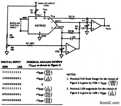
Bipolar_offset_binary_digital_to_voltage_converter_using_an_AD7520
Published:2009/7/20 3:41:00 Author:Jessie

Bipolar offset-binary digital-to-voltage converter (four-quadrant multiplier) using an AD7520. R1 and R2 are used for gain adjustment (courtesy Analog Devices, Inc.). (View)
View full Circuit Diagram | Comments | Reading(1295)
Voltage_to_frequency_convener
Published:2009/7/20 3:40:00 Author:Jessie
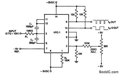
Voltage-to-frequency convener. Full scale frequency is 10 kHz as shown. The chip is the Datel VFQ-1 Not the fo output and fo/2 outputs. Full scale output can be extended to 100 kHz by changing C1 and C2 as indicated on schematic (courtesy Datel Systems, Inc.). (View)
View full Circuit Diagram | Comments | Reading(1031)
10_kHz_frequency_to_voltage_convener
Published:2009/7/20 3:39:00 Author:Jessie

10 kHz frequency-to-voltage convener. The input signal should be a pulse train or square wave with characteristics similar to TTL or 5-volt CMOS outputs. Minimum pulse width is 40 μs. Full scale output is 1 volt for a 10kHz input. To trim first set Vos to midrange and trim the 2K pot for 1-volt output. Then apply a 10-hertz waveform and trim Vos for a 10 mV output (courtesy Analog Devices, Inc.). (View)
View full Circuit Diagram | Comments | Reading(1096)
Sign_magnitude_DIA_converter_with_BCD_coding
Published:2009/7/20 3:38:00 Author:Jessie
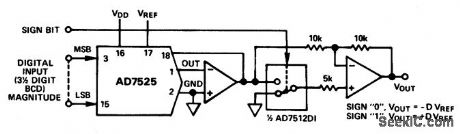
Sign-magnitude DIA converter with BCD coding. The AD7525 is used to provide a choice of positive or negative gains for the analog input signal, with sign-magnitude BVD coding. Gains range from -1.999 to +1.999. The BCD coding of the AD7525 permits it to be used with thumbwheel switches for manual gain setting without BCD-binary translation (courtesy Analog Devices, Inc.). (View)
View full Circuit Diagram | Comments | Reading(1245)
High_performance_RMS_to_DC_converter
Published:2009/7/20 3:36:00 Author:Jessie
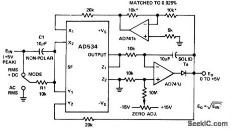
High-performance RMS-to-DC converter. To calibrate switch to RMS+DC,apply an input of say 1.00 volt DC and set the zero adjust until the output reads the same as the input.Check the inputs of ±5 volts(courtesy Analog Devices,Inc.). (View)
View full Circuit Diagram | Comments | Reading(1152)
Picoampere_to_voltage_converter_with_gain
Published:2009/7/20 3:35:00 Author:Jessie
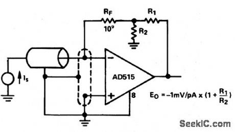
Picoampere-to-voltage converter with gain (courtesy Analog Devices, Inc.). (View)
View full Circuit Diagram | Comments | Reading(1021)
Current_to_voltage_converter_with_grounded_bias_and_sensor
Published:2009/7/20 3:34:00 Author:Jessie
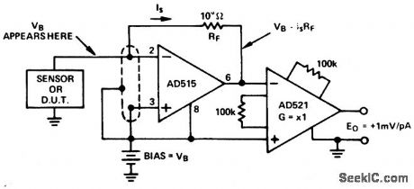
Current-to-voltage converter with grounded bias and sensor (courtesy Analog Devices, Inc.). (View)
View full Circuit Diagram | Comments | Reading(0)
| Pages:5/24 1234567891011121314151617181920Under 20 |
Circuit Categories
power supply circuit
Amplifier Circuit
Basic Circuit
LED and Light Circuit
Sensor Circuit
Signal Processing
Electrical Equipment Circuit
Control Circuit
Remote Control Circuit
A/D-D/A Converter Circuit
Audio Circuit
Measuring and Test Circuit
Communication Circuit
Computer-Related Circuit
555 Circuit
Automotive Circuit
Repairing Circuit