
A/D-D/A Converter Circuit
Index
Constituted by the INA118 differential voltage - current converter
Published:2014/5/21 20:31:00 Author:lynne | Keyword: Constituted by the INA118 differential voltage - current converter, INA118
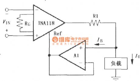
Constituted by the INA118 differential voltage - current converter circuit as shown:
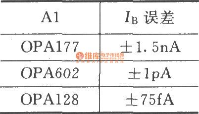
As shown by INA118 constitute differential voltage - current converter. INA118 current source constituted by the output of R1 and A1, due to high input impedance of the operational amplifier, the bias current is extremely small, and the output current to the load is negligible compared to, so the output current Io can be considered constant, and only the input voltage and R1 concerned that Io = (VIN/R1) × G. A1 Selection and IB error below. >The current source output current Io within a certain range regardless of the load, the input voltage and depends only on the resistors R1, when R1 is fixed, the output current and the input voltage VIN related only to complete the differential voltage - current conversion.
(View)
View full Circuit Diagram | Comments | Reading(7847)
Configured INA155/156 directly driven by a capacitive input high speed A / D converter
Published:2014/5/15 21:33:00 Author:lynne | Keyword: Configured INA155/156 directly driven by a capacitive input high speed A / D converter, INA155, INA156, ADS7818, ADS7834
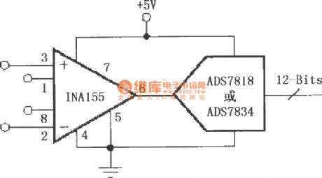
Configured INA155/156 directly driven by a capacitive input high speed A / D converter circuit as shown:
A capacitive high-speed direct drive input configured as shown in FIG INA155/156 by the A / D converter in Figure G = 10. After INA155 input voltage amplification to 12 high-speed low-power sampling A / D converter ADS7818 or ADS7834. ADS7818 or ADS7834 inputs for the internal capacitor array (CDAC), is the capacitive input, analog signal conversion A / D converter input is 12-bit digital signal output, fsample = 500kHz. (View)
View full Circuit Diagram | Comments | Reading(2282)
INA321/322 constituted by a direct drive capacitive input A / D converter
Published:2014/5/15 20:35:00 Author:lynne | Keyword: INA321/322 constituted by a direct drive capacitive input A / D converter, INA321, ADS7818, ADS7822
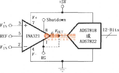
INA321/322 constituted by a direct drive capacitive input A / D converter circuit as shown:
As shown directly driving a capacitive input constituted by INA321/322 A / D converter. Since INA321/322 output is a low, so you can work at high frequencies directly drive capacitive loads. After INA321/322 amplified input voltage output, directly to the 12 high-speed low-power sampling A / D converter ADS7818 or ADS7822. ADS7818 or ADS7822 internal input terminal of the capacitor array (CDAC) digital-analog conversion, is a capacitive input, converts the analog signal A / D converter 12 converts the input digital signal output. (View)
View full Circuit Diagram | Comments | Reading(2117)
1.2 V voltage could be turned into 9 V converter circuit diagram
Published:2014/2/24 20:16:00 Author:lynne | Keyword: 1.2 V voltage could be turned into 9 V converter circuit diagram,
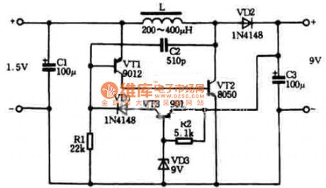
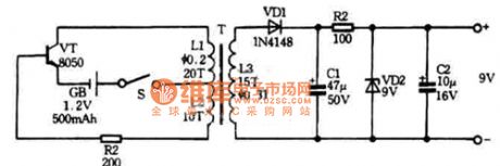
Figure 1 is a DC voltage boost circuit. The circuit can be a boost to 1.5V battery 9V, 9V laminated battery to replace. Circuit load input current is less than 1.2mA, the conversion efficiency up to 60%. The circuit consists of an oscillation circuit and voltage regulator circuit, which VT1, VT2, C2 composition oscillator, color code inductance L is the inductor, VD2 rectifier diode, C3 is the output filter capacitor, VT3, VD1, VD3 and R2 is stable the output voltage of the voltage regulator circuit. The output voltage is approximately equal to the value of VD3 of regulator. DC boost regulator circuit diagram shown in Figure 1
Figure 2 is a use of 1.2V, 500mAh nickel-cadmium batteries do power inverter circuit, the output voltage of 9V, digital multimeter available for use. Power inverter circuit shown in Figure 2
(View)
View full Circuit Diagram | Comments | Reading(4868)
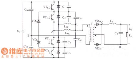
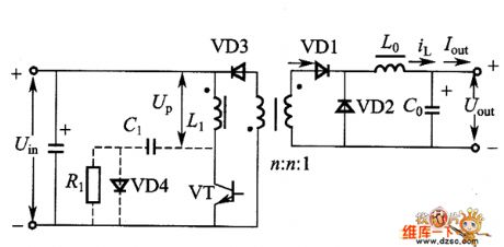
The basic three-level DC converter circuit diagram
Published:2014/1/23 21:16:00 Author:lynne | Keyword: The basic three-level DC converter circuit diagram,
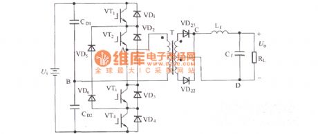
The basic three-level DC converter circuit diagram shown in Fig.:
(View)
View full Circuit Diagram | Comments | Reading(2380)
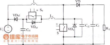
Zero-voltage switching three-level DC-DC converter circuit
Published:2014/1/23 20:30:00 Author:lynne | Keyword: Zero-voltage switching three-level DC-DC converter circuit,
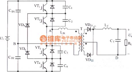
Zero-voltage switching three-level DC-DC converter circuit shown in Figure:
(View)
View full Circuit Diagram | Comments | Reading(2793)
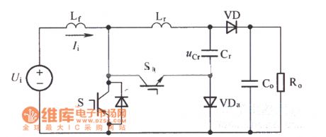
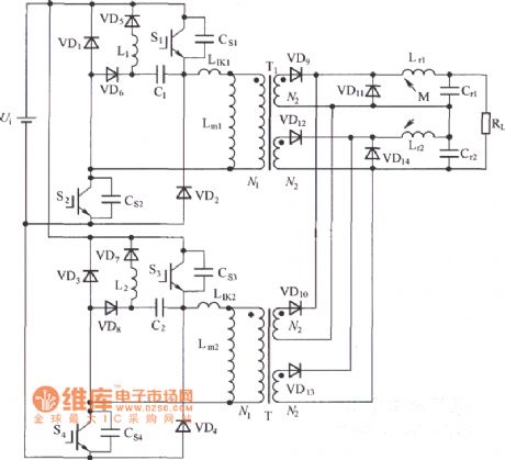
Wide load range three-level zero-voltage switching DC-DC converter circuit
Published:2014/1/23 20:27:00 Author:lynne | Keyword: Wide load range three-level zero-voltage switching DC-DC converter circuit,
Wide load range three-level zero-voltage switching DC-DC converter circuit shown in Figure:
(View)
View full Circuit Diagram | Comments | Reading(2006)
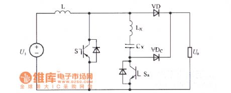
ZCZVT-PWM converter circuit
Published:2014/1/21 21:06:00 Author:lynne | Keyword: ZCZVT-PWM converter circuit,
ZCZVT-PWM converter circuit shown in Figure:
(View)
View full Circuit Diagram | Comments | Reading(1723)
Improved ZCT-PWM converter topology circuit
Published:2014/1/20 21:10:00 Author:lynne | Keyword: Improved ZCT-PWM converter topology circuit,
Improved ZCT-PWM converter topology circuit shown in Figure:
(View)
View full Circuit Diagram | Comments | Reading(1809)
Ordinary ZCT-PWM converter circuit diagram
Published:2014/1/20 20:28:00 Author:lynne | Keyword: Ordinary ZCT-PWM converter circuit diagram,
Ordinary ZCT-PWM converter circuit diagram shown in figure:
(View)
View full Circuit Diagram | Comments | Reading(1851)
Double-barrelled forward converter circuit topology circuit diagram
Published:2014/1/5 20:10:00 Author:lynne | Keyword: Double-barrelled forward converter circuit topology circuit diagram,
Double-barrelled forward converter circuit topology circuit diagram shown in Figure:
(View)
View full Circuit Diagram | Comments | Reading(2244)
Forward type ZVT - PWM converter main circuit principle diagram
Published:2014/1/5 20:05:00 Author:lynne | Keyword: Forward type ZVT - PWM converter main circuit principle diagram,
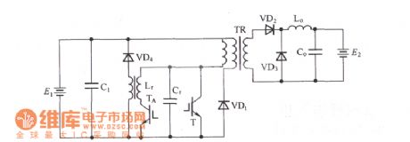
Forward type ZVT - PWM converter main circuit principle diagram as shown:
(View)
View full Circuit Diagram | Comments | Reading(1926)
Quasi-resonant soft-switching flyback converter schematic circuit
Published:2014/1/5 20:02:00 Author:lynne | Keyword: Quasi-resonant soft-switching flyback converter schematic circuit,
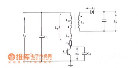
Quasi-resonant soft-switching flyback converter schematic circuit shown in Figure:
(View)
View full Circuit Diagram | Comments | Reading(2680)
Double Forward Converter circuit
Published:2013/12/12 20:17:00 Author:lynne | Keyword: Double Forward Converter circuit,
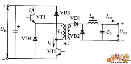
Double Forward Converter circuit shown in Figure:
(View)
View full Circuit Diagram | Comments | Reading(2313)
Single tube forward converter circuit diagram
Published:2013/12/12 20:18:00 Author:lynne | Keyword: Single tube forward converter circuit diagram,
Single tube forward converter circuit diagram shown in Fig.:
(View)
View full Circuit Diagram | Comments | Reading(1813)
LF355 Circuit
Published:2013/11/27 21:09:00 Author:lynne | Keyword: LF355 Circuit
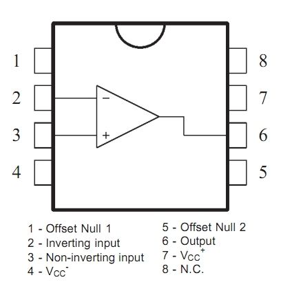
LF355 circuits are monolithic J-FET input operational amplifiers incorporating well matched, high voltage J-FET on the same chip with standard bipolar transistors. This amplifiers feature low input bias and offset currents, low input offset voltage and input offset voltage drift, coupled with offset adjust which does not degrade drift or common-mode rejection.
The devices are also designed for high slew rate, wide bandwidth, extremely fast settling time, low voltage and current noise and a low 1/f noise level.
LF355 typical applications
precision high speed integrators
fast D/A and converters
high impedance buffers
wideband, low noise, low drift amplifiers
logarithimic amd photocell amplifiers
sample and hold circuits (View)
View full Circuit Diagram | Comments | Reading(2375)
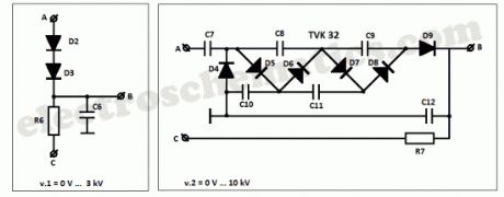
High Voltage Converter Circuits
Published:2013/11/27 21:01:00 Author:lynne | Keyword: High Voltage Converter Circuits
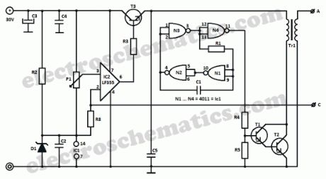
Starting from a 30 volt power supply this high voltage converter circuit can deliver a voltage between 0 to 3 kV (version 1) or from 0 to 10 kV (version 2).IC 4011 gates N1 … N3 are connected as astable multivibrator that commands the Darlington T1/T2 with an rectangular impulse of 20 kHz.
The transistors cannot be brought to saturation because of the low current that goes through them which will result in a very short block period. The rapid blocking of the transistors will produse an impulse of almost 300 V in the transformer’s T1 primary winding. This voltage is multiplied by the numbers of turns from the secondary winding.
For the first version it uses a monophased rectification. The second one uses a cascade rectifier from an old TV set and it delivers a 3 times higher voltage.
3 kV/10 kV High-Voltage Converter Schematic
Version 1 and 2 of the voltage converter
IC2 LF355 regulates the output voltage by comparing the P1′s voltage with that from the common point of the voltage divider R6/R8 or R7/R8. If the output outreaches the established voltage level, IC2 will reduce the supply voltage from the output through T3.
The most important part of the high voltage converter is the transformer. You may use a variety of cores E, E+I or ferrite with 30 mm diameter. The core must not have any air gap and a value for Al of 2000 nH is pretty good. The primary winding consists of 25 turns of 0.7 … 1 mm enamelled copper and the secondary winding consists of 500 turns of 0.2 … 0.3 mm conductor. Both of the windings must have very good insulation from each other.
Regarding this high voltage converter, please remember:
capacitor C6 must support a voltage of at least 3 kV
R6 at version 1 is made of six 10 MΩ resistors in series. R7 is made of six 50 MΩ resistors in series. This is done in order to eliminate the voltage spikes.
Each circuit consumes avout 50 mA without the load and 350 mA with a 2 … 3 W load. T2 and T3 transistors need good heatsinks.
Components list of the high voltage converterR1 = 4.7KR2 = R5 = 1KR3 = 330R4 = 2.7KR6 = 60MR7 = 300MP1 = 500K
C1 = 10nC2 = C4 = C5 = 100nC3 = 1000µFC6 = 10n / 3kVC7 …. C12 = from tv module TVK 32
D1 = Zener 11VD2 = D3 = BY127D4 …. D9 = from tv module TVK 32
T1 = 2N3055T2 = BF259T3 = BU208
Tr1 = read the article
IC1 = 4011IC2 = LF355
google_ad_client= ca-pub-9265205501290597 ;google_ad_slot= 6648404198 ;google_ad_width=336;google_ad_height=280;