
A/D-D/A Converter Circuit
Index 18
SWITCHING_REGULATOR_CONVERTER
Published:2009/6/26 4:00:00 Author:May
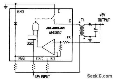
The Max650 switching regulator produces a regulated 5 V from large negative voltages, such as the -48 V found on telephone lines. The resulting power supply operates with several extemal com-ponents, inclucting a transformer, and it delivers 250 mA. The device includes a 140-V 250-mA pnp transistor, short-circuit protection, and all necessary control circuitry. (View)
View full Circuit Diagram | Comments | Reading(904)
V_F_CONVERTER
Published:2009/6/26 3:56:00 Author:May
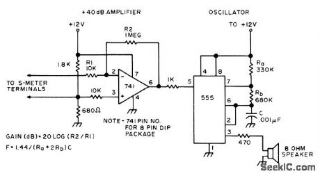
Voltage developed across Smeter is amplified by 741 opamp having gain of 40 dB so full.scale voltage of 100mV becomes 10V at opamp outptit. This drives modulation input of 555 timer connected as freerunning oscillator. Nominal 1-kHz output increases in frequency as drive current is reduced; conversely, drop in frequency corresponds to stronger signal at S-meter. Developed for use as audible guide when tuning Yagi and other beam antennas for amateur radio operation.-G.Hinkle, Closed Loop Antenna Tuning, 73 Magazine, May 1976, p 32-33. (View)
View full Circuit Diagram | Comments | Reading(1)
SIMPLE_LF_CONVERTER
Published:2009/6/26 3:44:00 Author:May

This converter allows coverage from 25 kHz up to 500 kHz. Use short coax from the converter to receiver antenna input. Tune the receiver to 3.5 MHz, peak for loudest crystal calibrator and tune your receiver higher in frequency to 3.6 MHz and you're tuning the 100 kHz range. 3.7 MHz puts you at 200 kHz, 3.8 MHz equals 300 kHz, 3.9 MHz yields 500 kHz, and 4.0 MHz gives you 500 kHz. (View)
View full Circuit Diagram | Comments | Reading(0)
INDUCTORLESS_POWER_SUPPLY_CONVERTER
Published:2009/6/26 3:39:00 Author:May
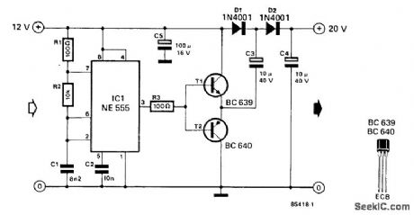
Using a 555 timer and voltage doubler, this circuit will supply ≥50mA at 20 Vdc. T1 and T2 act as power amplifiers to drive the voltage doubler. Frequency of operation is approximately 8.5 kHz. (View)
View full Circuit Diagram | Comments | Reading(3453)
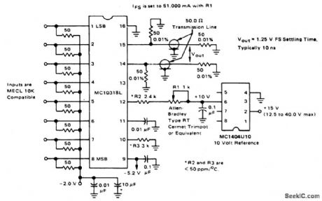
HIGH_SPEED_VOLTAGE_OUTPUT_DAC
Published:2009/6/26 2:57:00 Author:Jessie

View full Circuit Diagram | Comments | Reading(1705)
±10_V_FULL_SCALE_UNIPOLAR_DAC
Published:2009/6/26 2:51:00 Author:Jessie
View full Circuit Diagram | Comments | Reading(1684)
16_BIT_BINARY_DAC
Published:2009/6/26 2:43:00 Author:Jessie
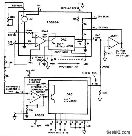
View full Circuit Diagram | Comments | Reading(1656)
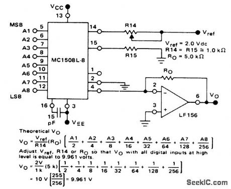
8_BIT_D_A_WITH_OUTPUT_CURRENT_TO_VOLTAGE_CONVERSION
Published:2009/6/26 2:40:00 Author:Jessie
View full Circuit Diagram | Comments | Reading(1627)
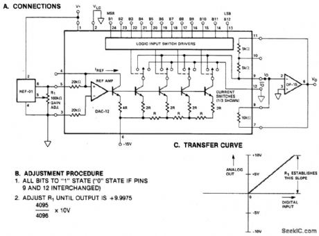
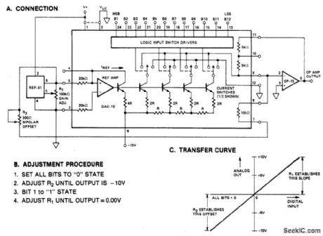
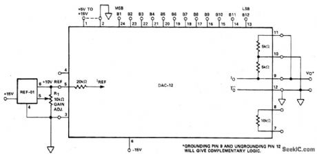
PRECISION_12_BIT_D_A_CONVERTER
Published:2009/6/26 2:35:00 Author:Jessie

View full Circuit Diagram | Comments | Reading(2377)
HIGH_SPEED_VOLTAGE_OUTPUT_DAC
Published:2009/6/26 2:57:00 Author:May
View full Circuit Diagram | Comments | Reading(0)
±10_V_FULL_SCALE_UNIPOLAR_DAC
Published:2009/6/26 2:51:00 Author:May
View full Circuit Diagram | Comments | Reading(0)
16_BIT_BINARY_DAC
Published:2009/6/26 2:43:00 Author:May
View full Circuit Diagram | Comments | Reading(0)
8_BIT_D_A_WITH_OUTPUT_CURRENT_TO_VOLTAGE_CONVERSION
Published:2009/6/26 2:40:00 Author:May
View full Circuit Diagram | Comments | Reading(0)
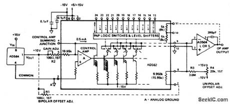
±10_V_FULL_SCALE_BIPOLAR_DAC
Published:2009/6/26 2:37:00 Author:May
View full Circuit Diagram | Comments | Reading(0)
PRECISION_12_BIT_D_A_CONVERTER
Published:2009/6/26 2:35:00 Author:May
View full Circuit Diagram | Comments | Reading(0)
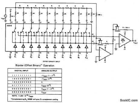
10_BIT,4_QUADRANT_MULTIPLEXING_D_A_CONVERTER(OFFSET_BINARY_CODING)
Published:2009/6/26 2:29:00 Author:May
View full Circuit Diagram | Comments | Reading(965)
HIGH_SPEED_8_BIT_D_A_CONVERTER
Published:2009/6/26 2:23:00 Author:May
View full Circuit Diagram | Comments | Reading(966)
8_BIT_D_A_CONVERTER
Published:2009/6/26 2:21:00 Author:May

View full Circuit Diagram | Comments | Reading(1309)
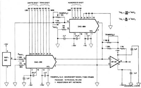
THREE_DIGIT_BCD_D_A_CONVERTER
Published:2009/6/26 2:17:00 Author:May
View full Circuit Diagram | Comments | Reading(891)
RESISTOR_TERMINATED_DAC0_TO_5_V_OUTPUT
Published:2009/6/26 2:15:00 Author:May
View full Circuit Diagram | Comments | Reading(950)
| Pages:18/24 1234567891011121314151617181920Under 20 |
Circuit Categories
power supply circuit
Amplifier Circuit
Basic Circuit
LED and Light Circuit
Sensor Circuit
Signal Processing
Electrical Equipment Circuit
Control Circuit
Remote Control Circuit
A/D-D/A Converter Circuit
Audio Circuit
Measuring and Test Circuit
Communication Circuit
Computer-Related Circuit
555 Circuit
Automotive Circuit
Repairing Circuit