
A/D-D/A Converter Circuit
Index 12
MULTIPLEXED_A_D_D_A_CONVERTER_INTER_FACE
Published:2009/7/7 5:20:00 Author:May

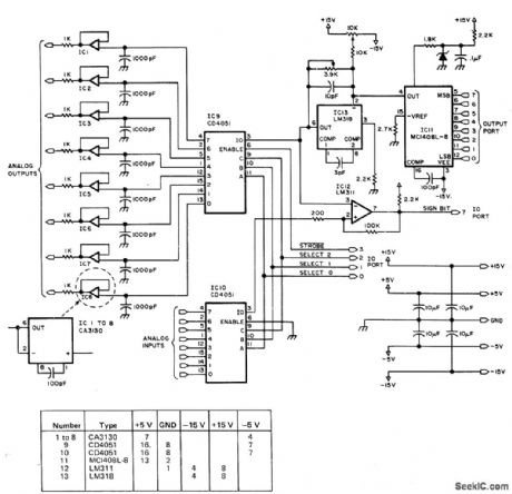
Time-multiplexed interface minimizes hardware required for applications of personal computer system. Useful in interactive games, equipment testing, and electronic music. Optimized for 0.1-100 Hz signals, Bypass each power pin with 0.01μF to suppress stray spikes caused by power surges. Use of LM318 opamp minimizes response time of MC1408L-8 DAC.-D. R. Kraul, Designing Multichannel Analog Interfaces, BYTE, June 1977, p 18-23. (View)
View full Circuit Diagram | Comments | Reading(2371)
CHARGE_DISPENSING_V_F_CONVERSION
Published:2009/7/7 4:55:00 Author:May
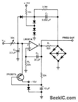
Output state of opamp switches C1 between reference voltage provided by diode bridge and its inverting input. Network R2-C2 reinforces direction of opamp output change. Circuit can deliver 0-10 kHz output with 0.01% linearity for 0-10 V input. -J. Williams, Low-Cost, Linear A/D Conversion Uses Single-Slope Techniques, EDN Magazine, Aug, 5, 1978, p 101-104. (View)
View full Circuit Diagram | Comments | Reading(974)
ISOLATED_15_V_DC_DC_CONVERTER
Published:2009/7/7 4:40:00 Author:May
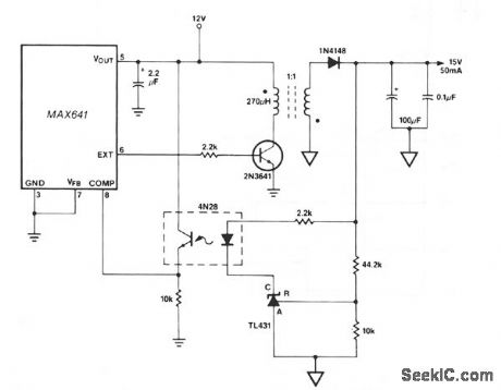
In this circuit, a TL431 shunt regulator is used to sense the output voltage. The TL431 drives the LED of a 4N28 optocoupler which provides feedback to the MAX641 while maintaining isolation between the input, + 12 V, and the output, + 15 V. In this circuit, the + 15 V output is fully regulated with respect to both line and load changes.
(View)
View full Circuit Diagram | Comments | Reading(3217)
SHORTWAVE_CONVERTER
Published:2009/7/7 4:38:00 Author:May
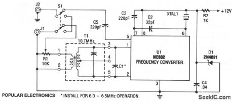
The NE602, U1, contains oscillator and mixer stages. The mixer combines the oscillator signal with the input rf signal to produce signals whose frequencies are the sum and difference of the input frequencies. For example, a 7.5-MHz signal is picked up by the antenna and mixes with the 8.5-MHz oscillator frequency. The difference between those two signals is 1 MHz-right in the center of your AM dial. Trans-former T1 is a 10.7-MHz i-f transformer. (View)
View full Circuit Diagram | Comments | Reading(1086)
4_18MHZ_CONVERTER
Published:2009/7/7 4:37:00 Author:May
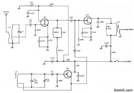
The unit consists of rf amplifier Q1, local oscillator Q2, and mixer Q3. The two bands are covered without a bandswitch by using an i-f or 3.5 MHz. The oscillator range is 7.5 to 14.5 MHz. Incoming signals from 4 to 11 MHz are mixed with the oscillator to produce the 3.5-MHz i-f. Signals from 11 to 18 MHz are mixed with the oscillator to also produce an i-f of 3.5 MHz. At any one oscillator frequency, the two incoming signals are 7 MHz apart. Rf amplifier input C1/L1 comprises a high-Q, lightly loaded, tuned circuit; this is essential for good band separation. (View)
View full Circuit Diagram | Comments | Reading(1163)
VOLTAGE_TO_CURRENT
Published:2009/7/7 4:34:00 Author:May
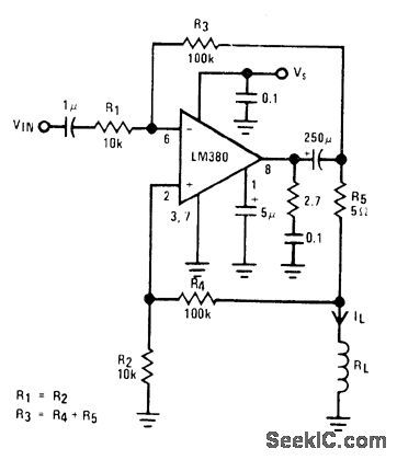
Circuit is capable of supplying constant alternating current up to 1 A to variable load. Actual value of load current is determined by input voltage, values of R1-R3, and value of R5. Input of 250 mV gives 0.5 A through load (RMS values) with less than 0.5% total harmonic distortion. Applications include control of electromagnet current.- Audio Handbook, National Semiconductor, Santa Clara,CA,1977, p 4-21-4-28. (View)
View full Circuit Diagram | Comments | Reading(960)
DIGITAL_TO_FREQUENCY
Published:2009/7/7 4:26:00 Author:May
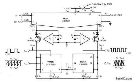
Combination of multiplying DAC and 556 dual timer provides complementary output frequencies under con trol of digital input. Opamp and diode types are not critical. Output frequency of each timer depends on supply voltages, capacitor values,and setting of R1.-J. Wilson and J. Whitmore,MDAC's Open Up a New World of Digital-Control Applications,EDN Magazine,Sept.20、1978、p 97-105. (View)
View full Circuit Diagram | Comments | Reading(905)
LOW_FREQUENCY_CONVERTER
Published:2009/7/7 4:23:00 Author:May
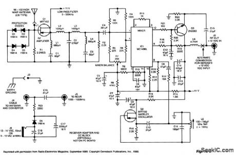
Among the signals below 550 kHz are maritime mobile,distress,radio beacons,aircraft weather,European Longwave-AM broadcast, and point-to-point communications. The low-frequency converterconverts the 10to 500 kHz LW range to a 1010 to 1550 kHz MW range,by adding 1000 kHz to all received signals,Radio calibration is unnecessary because signals are received at the AM-radio's dial setting,plus 1MHz;a 100-kHz signal is received at 1100 kHz,a 335-kHz signal at 1335 kHz,etc.The low-frequencysignals are fed to IC1,a doubly-balanced mlxer.
Transistor Q2 and associated circuitry form a Hartley 1000-kHz local oscillator, which is coupled from Q2's drain,through C8,to IC1 pm 8.Signals in the 10-550 kHz range are convened to 1010-1550 kHz.The mixer heterodynes the mcommg low-frequency signal and local-oscillator signal.Transistor Q3reduces IC1's high-output impedance to about 100 Ω to match most recelver inputs.Capacitor C15 couples the 1010-1550 kHz frequencies from Q3's emitter to output jack J3,while blocking any dc bias.
Inductor L6 couples the dc voltage that's carried h the rf signal cable from the rcvr/dc adaptor. The dc voltage and rf signals don't interfere with one another;that saves runmng a separate power-supply wire,which simplifies installation at a remote location.Capacitors C14 and C13 provide dc supply filtering.Thekit is available from North Country Radio,P.O.Box 53,Wykagyl Station,NY 10804.
(View)
View full Circuit Diagram | Comments | Reading(0)
PLL_clock_for_a_ADC1100_BCD_dual_slope_A_D_convener
Published:2009/7/21 23:16:00 Author:Jessie
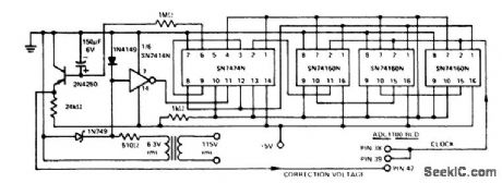
PLL clock for a ADC1100/BCD dual-slope A/D convener (courtesy Analog Devices, Inc.). (View)
View full Circuit Diagram | Comments | Reading(1241)
Count_by_5_counter_using_an_ADC1100_dual_slope_A_D_convener
Published:2009/7/21 22:05:00 Author:Jessie
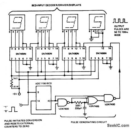
Count-by-5 counter using an ADC1100 dual-slope A/D convener (courtesy Analog Devices, Inc.). (View)
View full Circuit Diagram | Comments | Reading(1529)
FET_TRIANGLE_TO_SINE_CONVERTER
Published:2009/7/6 22:18:00 Author:May
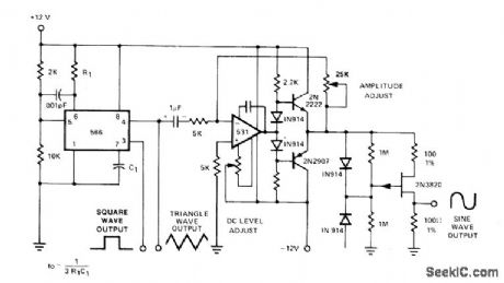
Use of nonlinear transfer characteristic of P-channel junctidn FET to shape triangle outρut of 566 function generator gives sine wave having less than 2% distortion. Amplitude of triangle wave is critical and must be carefully adjusted for minimum distortion of slne output.-''Signetics Analog Data Manual,''Signetics,Sunnyvale,CA,1977,p 851-852 (View)
View full Circuit Diagram | Comments | Reading(3327)
TRIANGLE_TO_SINE_CONVERTE
Published:2009/7/6 21:39:00 Author:May
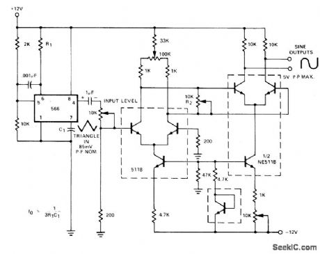
Nonlinear emitter-base junction characteristic of 511B transistorarray is used for shaping triangle output of 566 function generator to give sine output having less than 2% distortion. Amplitude of triangle is critical and must be carefully adjusted for minimum distortion of sine wave by varying values of R1, R2, and input level pot while monitoring output with Hewlett-Packard 333A distortion analyzer.- Signetics Analog Data Manual, Signetics, Sunnyvale, CA, 1977, p 851-853. (View)
View full Circuit Diagram | Comments | Reading(1159)
PARALLEL_TO_SERIAL__CONVERTER
Published:2009/7/6 21:24:00 Author:May
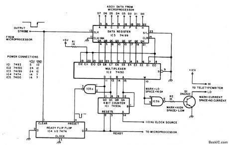
Multiplexer IC2 selects formatting and data bits according to state of IC1, IC3 is output latch Teletypewriter current loop is driven by Q1 from output of multiplexer. 110-Hz clock gives transfer rate of 10 characters per second. Provides standard asynchronous format of 1 start bit, 8 data bits, and 2 stop bits for teletypewriter without using universal asynchronous receiver-transmitter,-G. C. Jewell, How to Drive a Teletype Without a UART, BYTE, Jan, 1977, p 32. (View)
View full Circuit Diagram | Comments | Reading(2619)
8_bit_D_A_converter_with_microprocessor_interface
Published:2009/7/23 21:39:00 Author:Jessie
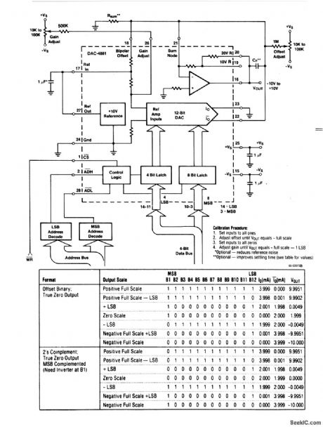
This circuit uses a DAC-4881 and a few external components to form a D/A converter with microprocessor interface (8-bit data bus). The output is + 10 V to -10 V with complementary binary input (all zeros equal full scale). (View)
View full Circuit Diagram | Comments | Reading(935)
Simple_fast_10_bit_A_D_converter
Published:2009/7/22 21:59:00 Author:Jessie
This circuit is especially useful where a large number of converters is required and all can be serviced by one clock. For a 0-2.5-V range, the analog input (EX) is applied to the 2.5-kΩ resistor. For a 0-to 10-V range, the 2.5-kΩ resistor is grounded and EX is applied to the 7.5-kΩ resistor. The 100-MHz clock pulse bursts that appear at the output are proportional to EX. For a 0- to 10-V input, 1024 pulses appear at full-scale, 512 pulses at 5.00 V etc. The circuit will hold ±1 LSB accuracy over 0°C to 70°C with an additional t1 LSB uncertainty. The 2-kΩ gain trim pot is adjusted for the desired output count. (View)
View full Circuit Diagram | Comments | Reading(1100)
Fully_isolated_10_bit_A_D_converter
Published:2009/7/22 21:56:00 Author:Jessie
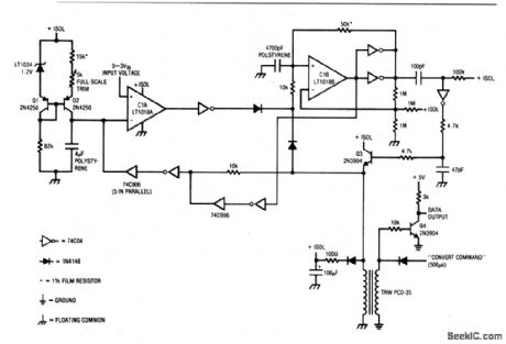
This circuit is fully floating from system ground, and is ideal for performing A/D conversion in the face of the high common-mode noise characteristics of predominantly digital systems. The circuit is also useful in industrial environments where noise and high common-mode voltages are present in transducer-fed systems. To calibrate, apply 3.000 V at the input, and trim the 5-kΩ pot for 1024 counts at the data output (Q4 collector). (View)
View full Circuit Diagram | Comments | Reading(837)
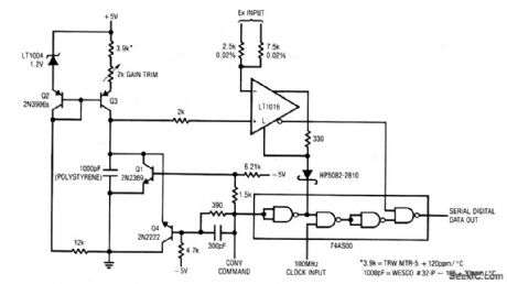
Microporoer_12_bit_A_D_converter
Published:2009/7/22 21:53:00 Author:Jessie
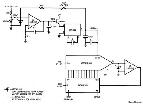
This A/D converter has a 300-μs conversion time, consumes only 890 μA, with a temperature coefficient of 30 ppm/°C and an accuracy of ±2 LSBs. To calibrate, adjust the 100-kΩ pot for exactly -5V at VREF (pin 5 of the LTC1044). No further adjustment is necessary. (View)
View full Circuit Diagram | Comments | Reading(1016)
01_1_100_and_1000_Hz_SINE_SQUARE_TRIANGLE_
Published:2009/7/6 20:47:00 Author:May
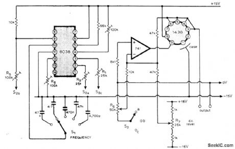
Provides choice of five spot frequencies switched in decades by S1. Setting of S2 determines shape of output waveform. Adjust R1, R2, and R3, to make peak-to-peak amplitudes of all three waveforms equal. R4, controls symmetry. R2 is adjusted for minimum distortion of sine-wave output. Output may be set up to 100 mA by R6, and is short-circuit-proof. DC level may be set anywhere between ±14 V by R7. Motorola 1438 IC and 741 opamp boost output of 8038 IC sufficiently to drive most laboratory loads.-G. R. Wilson, Low-requency Generator, Wireless World, Feb. 1977, p 44. (View)
View full Circuit Diagram | Comments | Reading(925)
FREQUENCY_TO_VOLTAGE_CONVERTER
Published:2009/7/6 20:23:00 Author:May
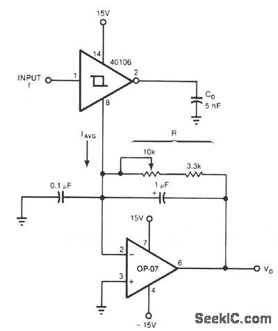
Six components can configure a circuit whose output voltage is proportional to its input frequency. The average current VAVG from the 40106 Schmitt trigger inverter's ground pin 8 is linearly dependent on the frequency at which C0 is discharged into the op amp's summing junction. The op amp forces this current to flow through the 13.33-KΩ feedback resistor, producing a corresponding voltage drop. This frequency-to-voltage converter yields 0 to -10 V output with 0 to 10 kHz input frequencies. (View)
View full Circuit Diagram | Comments | Reading(0)
1500_V_ISOLATION_FOR_DAC
Published:2009/7/6 7:51:00 Author:May
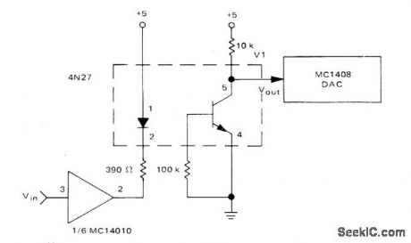
Motorola 4N27 optoisolator provides required isolation between DAC of programmable power supply and remotely located CMOS MC14010 noninverting buffer.-D. Aldridge and N. Wellenstein, Designing Digitally-Controlled Power Supplies, Motorola, Phoenix, AZ, 1975, AN-703, p 9. (View)
View full Circuit Diagram | Comments | Reading(1339)
| Pages:12/24 1234567891011121314151617181920Under 20 |
Circuit Categories
power supply circuit
Amplifier Circuit
Basic Circuit
LED and Light Circuit
Sensor Circuit
Signal Processing
Electrical Equipment Circuit
Control Circuit
Remote Control Circuit
A/D-D/A Converter Circuit
Audio Circuit
Measuring and Test Circuit
Communication Circuit
Computer-Related Circuit
555 Circuit
Automotive Circuit
Repairing Circuit