
A/D-D/A Converter Circuit
Index 3
16 bit Analogue to Digital Converter LTC1052
Published:2012/9/11 21:18:00 Author:Ecco | Keyword: 16 bit, Analogue to Digital , Converter
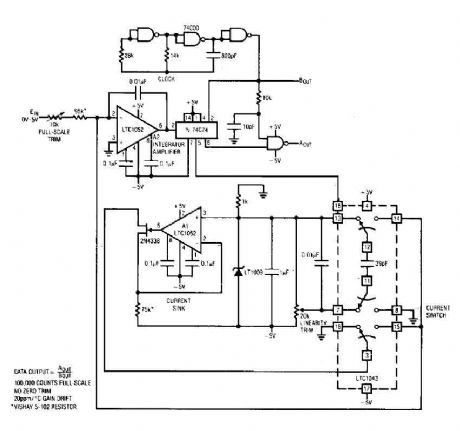
The circuit here is a A/D converter, that consisting of A2, a flip-flop, some doors and a current sink, is based on a current balancing technique. Again, the stabilized LTC 1052 50 no drift of V input 1 ° C is necessary to eliminate the offset errors of aid. (View)
View full Circuit Diagram | Comments | Reading(1835)
10 Bit A-D converter circuit
Published:2012/9/11 21:18:00 Author:Ecco | Keyword: 10 Bit , A-D converter
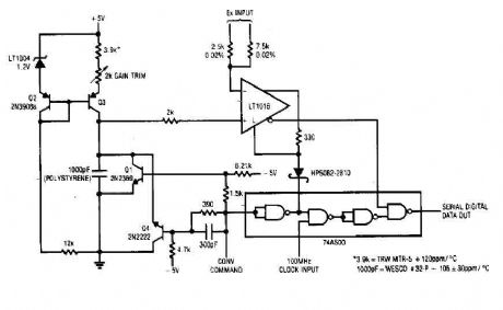
Each time a pulse is applied to the conversion of the control input, Ql resets the 1000 pF capacitor to 0 V. This action takes 200 ns to reset the falling edge of the convert command pulse, the capacitor begins to charge linearly. In exactly 10 microseconds, it loads to 2.5 V. The ramp is 10 microseconds applied to the positive input of the LTl016. The LT1016 compares the ramp Ex, the unknown, its negative input. For a 0 V - 2.5 V range, Ex is applied to the resistance of 2.5 k ohm. (View)
View full Circuit Diagram | Comments | Reading(1631)
A/D Converter with LT1018
Published:2012/9/11 21:18:00 Author:Ecco | Keyword: A/D Converter
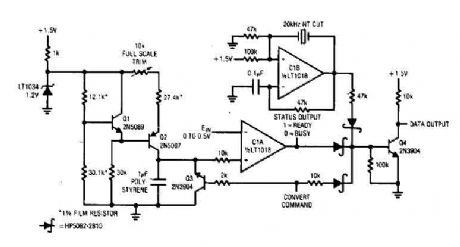
The converter has a 60-ms conversion consumes 460 pA of 1's. 5 V power supply and maintains an accuracy of 10 bits on a 15 ° C in the temperature range of 35 ° C. A pulse applied to convert the command line causes Q3, operating in reverse mode, the discharge path through the diode 10 kO, forcing its collector low. Q3 results of reverse mode switching in a capacitor discharge to 1 mV of ground. During the time of the ramp value is less than the input voltage, output of the CIA is low. (View)
View full Circuit Diagram | Comments | Reading(1502)
High Speed A/D converter 12-bit
Published:2012/9/11 21:17:00 Author:Ecco | Keyword: High Speed , A/D converter, 12-bit
This system performs a complete conversion of 12 bits in 10 p unipolar or bipolar. This converter is accurate to ± 12-bit LSB Y2 and a typical gain TC of 10 ppm / ° C. In unipolar mode, the system range is 0 V to 9.9976 V, with each bit having a value of 2.44 mY. For the accuracy of true conversion, an A / D converter must be trimmed so that, given the results just the exit code of input levels of Y2 Y2 LSB LSB below to above the exact voltage represents the code. (View)
View full Circuit Diagram | Comments | Reading(1416)
Simple A/D converter circuit with 2504
Published:2012/9/11 21:16:00 Author:Ecco | Keyword: Simple A/D converter
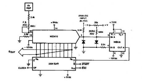
Time IO-bit conversion is 3.3 MHz with a p 3. Clock. This converter uses an approximation 2504 12-bit register in successive operating mode where the short-cycle end signal conversion is taken from the first bit used in the SAR (QLO). (View)
View full Circuit Diagram | Comments | Reading(1131)
14 Bit A-D Converter with ICL7134B
Published:2012/9/11 21:16:00 Author:Ecco | Keyword: 14 Bit , A-D Converter
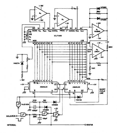
The circuit ICL7134B base is a bipolar input AID converter broadband, using two AM25L03s to form a successive approximation register 14-bit. The comparator is a circuit with two stage amplifier HA2605 front, used to reduce the settling time problems in the pro summing node (see A020). Warning nu11ing offset of this amplifier is needed and if wide temperature range operation is desired, an auto-zero circuit using a lCL7650 is probably desirable (see A053). The clock, using two gates TTL Schmitt trigger operates at a slower pace for the first 8 bits, where the settlement time is more critical than for the last 6 bits. (View)
View full Circuit Diagram | Comments | Reading(1490)
Cyclic A/D converter circuit
Published:2012/9/11 21:15:00 Author:Ecco | Keyword: Cyclic A/D converter
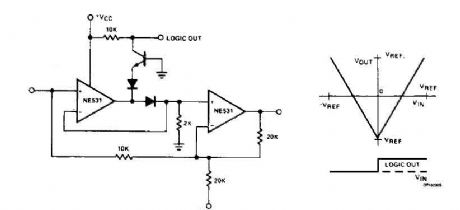
The cyclic converter consists of a chain of identical stages, each of which detects the polarity of the input. Step V REF then subtracted from the double entry and the rest if the polarity is correct. The signal is full wave rectified and the rest of V IN - V REF is doubled. (View)
View full Circuit Diagram | Comments | Reading(1050)
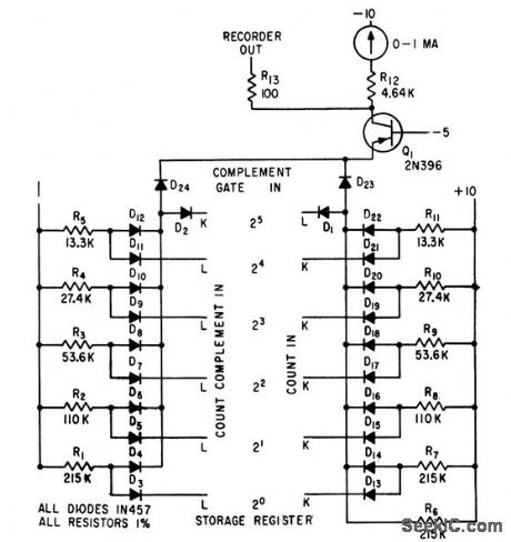
Differential A/D Converter circuit CA3110
Published:2012/9/11 21:15:00 Author:Ecco | Keyword: Differential, A/D Converter
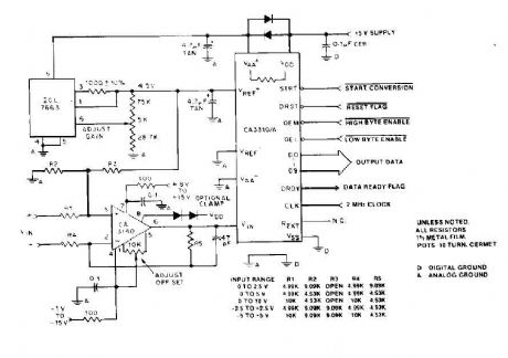
By using an op amp BiMOS CA3140 provides good orientation skills for high bandwidth signal input, and can quickly adjust the energy output at its terminal CA33IO WINE. The CA3140 can also lead to near the negative supply rail. (View)
View full Circuit Diagram | Comments | Reading(1699)
Isolated converter circuit diagram composed of LT1425
Published:2012/7/3 22:29:00 Author:Ecco | Keyword: Isolated converter
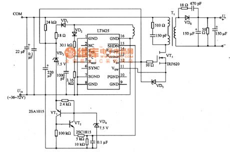
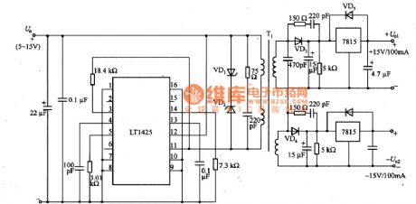
Figure a, b are the isolated converter circuit composed of LT1425. The input voltage of the circuit shown in Figure (a) is -36 ~-72V, and the output is 5V/2A. The LT1425 is an integrated circuit with current working way, and the oscillation frequency is 275kHZ. It has all the features required by the power supply circuit, and the leakage current of the on-chip switching power MOSFET is 1.5A . The circuit does not impose feedback, so the load adjustment rate is ± 5% . In order to increase the stability of the load changes and remove a part of voltage from the output to add to the feedback side, people enhancethe stability of the circuit.
Figure (b) is a dual-output converter circuit using LT1425. The circuit has no a negative feedback circuit, its output is added a three-terminal integrated regulator 7815 to increase stability. When the input voltage is 5V, the conversion efficiency is 72% ; when the input voltage is 15V, the conversion efficiency is 80% , and its isolation performance depends on the structure of the winding of transformer T1.
(View)
View full Circuit Diagram | Comments | Reading(1936)
Current resonance converter circuit diagram composed of NE555
Published:2012/7/3 22:13:00 Author:Ecco | Keyword: Current resonance converter
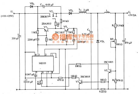
Figure 21 shows the current resonance converter circuit diagram composed of NE555. In the circuit, NE555 is the voltage controlled oscillator. MOSFET (VT1 ), freewheeling diode VD2 and smoothing inductor L1 constitute a common step-down DC / DC converter. L2 and C1 form the resonant circuit, VD2 is a diode to realize half-wave current resonance. VD1 and C3 form the bootstrap circuit to provide gate drive current for the the VT1. Voltage divider resistors R1 , R2 and RP1 are used to detect the output voltage, and the voltage is added to the VT5's base to control the frequency of the NE555. VT3 is the overcurrent protection circuit which can control the output current in the range of 0.5 ~ 3A.
(View)
View full Circuit Diagram | Comments | Reading(3131)
Voltage Three-phase Bridge and Push-pull Inverter Circuit
Published:2011/9/3 9:17:00 Author:Zoey | Keyword: Voltage, Three-phase, Bridge, Push-pull, Inverter Circuit
Voltage three-phase bridge and push-pull inverter circuit
In addition to the inverter output waveform performanceindex, Performance indicators should also include: Inverter efficiencyPower output bya unitofweight (or volume)Reliability index AC component value and pulse frequency of DC current input by the inverterElectromagnetic interference (EMI) and electromagnetic compatibility EMC Push-pull single-phase inverter circuit (View)
View full Circuit Diagram | Comments | Reading(1586)
High speed switching circuit composed of the SW-239
Published:2011/9/4 20:44:00 Author:TaoXi | Keyword: High speed, switching circuit
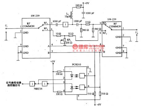
The High speed switching circuit composed of the SW-239 is as shown in the figure. This kind of circuit uses the high speed switch SW-239, and it switches the pathes of a few MHZ to several hundred megahertz high frequency signals. The switching speed is decided by the optocoupler PC9DlO. The SW-239 has the 50Ω resistance, the RFcircuit isalways in the open-circuit state before and after the switching, so it has very low coupling to the switch and the surround circuit, the switch conduction and the deadline isolation degree are very high. So when the circuit is switching, it will not produce the peak voltage pulse. RP1 can be used to adjust the gain (before and after the switching).
(View)
View full Circuit Diagram | Comments | Reading(1856)
RTTY_SPEED_CONVERTER
Published:2009/7/14 22:45:00 Author:Jessie
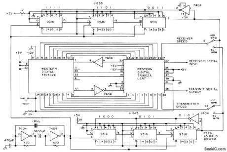
Digital speed converter for amateur RTTY permits transmitting either above or below input speed from key-board or tape Uses FR1502E 40-character 9-bitFIFO storage chip, TR1602A universal asynchronous receiver-transmitter, and six Fairchild 9316 programmable dividers. Values shown give choice of 60 or 100 WPM for receiving and for transmitting, derived by dividing down from same 1-MHz clock. Input and output are TTL-compatible.-A. Sperduti, The 60 WPM Conversion, 73 Magazine, April 1977, p 158-159. (View)
View full Circuit Diagram | Comments | Reading(1309)
WIDE_BANDWIDTH_VOLTAGE_TO_FREQUENCY_CONVERTER
Published:2009/7/14 22:47:00 Author:Jessie
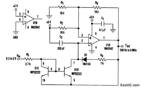
Shown is the design for a low-cost, wide-bandwidth voltage-to-frequency converter (VFC). The core element of the prototype VFC is a Maxim MAX942 high-speed comparator. When operating, R1, R2, and R3 provide hysteresis with trip points from one-third to two-thirds of the supply voltage.This permits wide adjustability in the width of the output pulse. Q1C and Q1B form a current mirror that linearizes the charge potential across C2. As the voltage at pin 2 of U1 crosses the lower trip point, the comparator output turns on. The current mirror sink node is raised above the program voltage, which turns it off. D1 turns on, removing the charge on C2 through R4. When the voltage at U1 pin 2 crosses the upper trip point, the circuit resets. Upon observation, the prototype circuit linearity was approximately 2 percent over the tested range. Also, up to 6-MHz operation was possible using the MAX942 by carefully selecting C2 and the hysteresis resistors. Discrete transistors can be used instead of the Motorola MPQ2N2222 monolithic quad package. This can cause some instability at low frequencies. The transistors should be located in close thermal proximity. On the high side, a good, matched transistor pair can be used. Analog Devices' MAT-01 is a good choice. (View)
View full Circuit Diagram | Comments | Reading(2498)
AC_DC_CONVERTER
Published:2009/7/15 1:37:00 Author:Jessie
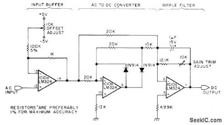
Used for measuring AC voltage with digital DC voltmeter, Besulting signal is equal to average RMS value of applied input signal. When 1-V peak 60-Hz is applied to converter, output should be +0.707 VDC. Connect pin 4 of LM324 to +5 V and pin 11 to -5 V.–S. Ciarcia, Add More zing to the Cocktail, BYTE, Jan 1978,p37-39, 44, 46, 48, 50-52, and 54. (View)
View full Circuit Diagram | Comments | Reading(4716)
WWV_CONVERTER
Published:2009/7/15 5:08:00 Author:Jessie
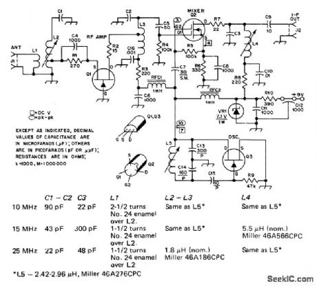
Designed for use with amateur receiver for reception of NBS stationsWWV or WWVH on 10, 15, or 25 MHz. Receiver is tuned to 4, 14, or 21 MHz to serve as IF amplifier, detector, and audio stages. Current drain of converter is 15 mA, low enough for operation from 9-V transistor-radio battery. Table gives tuned-circuit values for frequency desired. Restriction to single frequency eliminates band-switching. Q1 can be any commom-gate JFET RF amplifier providing 8-dB gain. Mixer is 40673 MOSFET. Oscillator transistor is not critical. Oscillator output serves for all three WWV frequencies. -C. Watts, NBS-Ears for Your Ham-Band Receivers, QST, June 1976, p 25-26. (View)
View full Circuit Diagram | Comments | Reading(0)
DIGITAL_ANALOG_CONVERTER
Published:2009/7/14 2:44:00 Author:May
Converts binary digits to analog form.-K,H. Brackney and D. R.Gosch, Pulse Comparator Circuit Measures Frequency Jitter,Elecytronics,34:27,p 54-56. (View)
View full Circuit Diagram | Comments | Reading(1334)
12_TO_162V_D_C_CONVERTER
Published:2009/7/13 19:57:00 Author:May
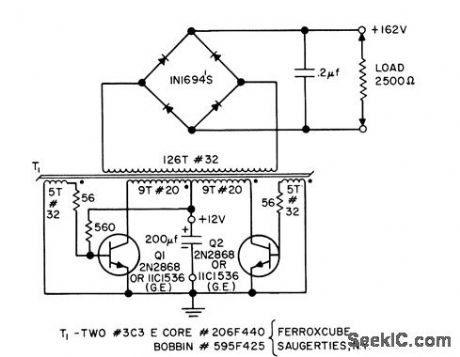
Simple and efficient saturating-core inverter provides 10w output with efficiency of 80%,using operating frequency of about 8.5kc,- Transistor Manual, Seventh Edition, General Electric Co.1964,p237 (View)
View full Circuit Diagram | Comments | Reading(1685)
2_m_TO_BROADCAST_BAND
Published:2009/7/16 3:52:00 Author:Jessie
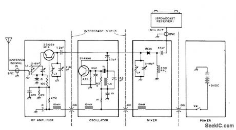
Permits tuning to 2-m (146-MHz) amateur band with ordinary AM auto radio, for monitoring FM repeaters and other 2-m amateur stations. Article stresses importance of shielding, compartmentalization, and RF blocking along power lead to prevent bleed-through of broadcast stations. Separate 9-V battery gives long life if converter is turned off when not in use, because drain is only 25 mA. L2 is 4 turns No. 20 on 7-mm slug-tuned form, with 2-turn link L1 at low end and tap 11/2 turns from low end. L3 and L4 are 3 turns No. 20 on 7-mm slug-tuned form. L5 is 20 turns No. 30 on 4-mm solid ferrite form. Y1 is 48.5-MHz third-overtone crystal. Convener gives good reception of both AM and FM stations on 2 m, with sharpness of receiver IF tuning determining ability of radio to slope-detect FM signals.-J. R. Johnson, New Improved Repeater Monitor, 73 Magazine. Dec. 1976, p 106-109. (View)
View full Circuit Diagram | Comments | Reading(1528)
WWV_ON_AC_DC_RADIO
Published:2009/7/16 3:50:00 Author:Jessie
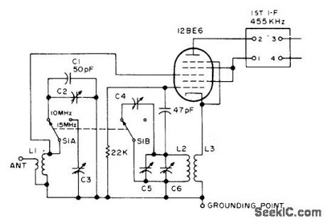
When fed into IF amplifier of ordinary broadcast-band radio, simple converter circuit gives choice of WWV on 10 or 15 MHz, for reception of time signals and radio propagation reports. C2 is 1.5-10 pF; C3 and C6 are 7-60 pF; C4 is 7-100 pF (all compression trimmers); and C5 is 1.8-8.7 pF miniature variable capacitor. -W. C. Powis, Notes on Converting the AC/DC for WWV, 73Magazine, Oct. 1974, p 116. (View)
View full Circuit Diagram | Comments | Reading(1340)
| Pages:3/24 1234567891011121314151617181920Under 20 |
Circuit Categories
power supply circuit
Amplifier Circuit
Basic Circuit
LED and Light Circuit
Sensor Circuit
Signal Processing
Electrical Equipment Circuit
Control Circuit
Remote Control Circuit
A/D-D/A Converter Circuit
Audio Circuit
Measuring and Test Circuit
Communication Circuit
Computer-Related Circuit
555 Circuit
Automotive Circuit
Repairing Circuit