
A/D-D/A Converter Circuit
Index 14
16_BIT_A_D_CONVERTER
Published:2009/7/2 3:50:00 Author:May
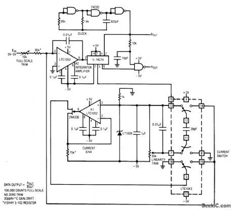
The A/D converter, made up of A2, a flip-flop, some gates and a current sink, is based on a current balancing technique. Once again, the chopper-stabilized LTC1052's 50 nV/℃ input drift is required to eliminate offset errors in the A/D. (View)
View full Circuit Diagram | Comments | Reading(1189)
4_DIGIT(10000_COUNT)A_D_CONVERTER
Published:2009/7/2 3:46:00 Author:May
View full Circuit Diagram | Comments | Reading(1010)
SUCCESSIVE_APPROXIMATION_A_D_CONVERTERS
Published:2009/7/2 3:42:00 Author:May
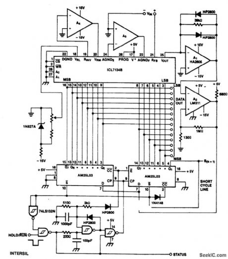
The ICL7134B-based circuit is for a bipolar-input high-speed A/D converter, using two AM25L03s to form a 14-bit successive approximation register. The comparator is a two-stage circuit with an HA2605 front-end amplifier, used to reduce settling time problerns at the summing node (see A020). Careful offset-nulling of this amplifier is needed, and if wide temperature range operation is desired, an auto-null circuit using an ICL7650 is probably advisable (see A053). The clock, using two Schmitt trigger TTL gates, runs at a slower rate for the first 8 bits, where settling-time is most critical than for the last 6 bits. The short-cycle line is shown tied to the 15th bit; if fewer bits are required, it can be moved up accordingly. The circuit will free-run if the HOLD/RUN input is held low, but will stop after completing a conversion if the pin is high at that time. A lowgoing pulse will restart it. The STATUS output indicates when the device is operating, and the falling edge indicates the availability of new data. A unipolar version can be constructed by typing the MSB (D13) on an ICL7134U to pin 14 on the first AM25L03, deleting the reference inversion amplifier A4, and tying VRFM to VRFL. (View)
View full Circuit Diagram | Comments | Reading(2040)
-10_V_GIVES_10_kHz
Published:2009/7/2 3:00:00 Author:May
Control voltage input in range of 0 to -10 V is converted linearly to frequency of digital output pulse train haiving fullscale value of 10 kHz. Internal regulation of circuit makes operation essentially independent of ±15 V supply level.A1 is opamp integrator, A2 is comparator, and A3 is precision mono MVBR. Transistor switch Q1 connects Rb to 3.15-V reference voltage during t1 timing period of A3.—W.G.Jung, IC Timer Cookbook, Howard W.Sams, Indianapolis, IN, 1977, p184-192 (View)
View full Circuit Diagram | Comments | Reading(0)
F_V_CONVERTER_
Published:2009/7/1 23:46:00 Author:May
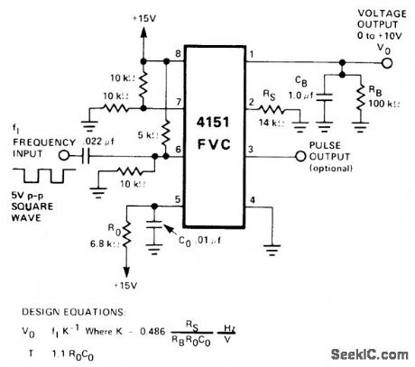
Single-suρply circuit uses frequency-to-voltage connection of RM4151converter to make output voltage vary between 0 and as frequency of 5 V P-P squarewave inρut varles bettween 0 and 10 kHz,-″Linear Integrated Circuit Data Book,'' RaytheonSemiconductor Division,Mountain View,CA, 1978,p 7-39. (View)
View full Circuit Diagram | Comments | Reading(1539)
CLICKING_METRONOME
Published:2009/7/1 22:19:00 Author:May
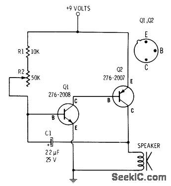
Basic lamp-flashing circuit iS used to produce sharp click In loudspeaker each time Q2 is turned on by RC oscillator Q1 R2 adjusts repetition rate over range of 20-280 beats per minute Changing value of C1 varies tone of clicks.-F M Mims.″Transistor Projects,vol.1. Radio Shack.Fort Worth.TX.1977.2nd Ed,p 33-39. (View)
View full Circuit Diagram | Comments | Reading(968)
12_BIT_DAC_WITH_VARIABLE_STEP_SIZE
Published:2009/7/1 21:31:00 Author:May
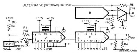
The step size of the converter is variable by selection of the high order data bits.The first DAC, A, has a stable reference current supplied via the 10.24 V reference IC and R1. R2 provides bias cancellation. As shown, only the first 4 MSB inputs are used, giving a step size of225/256 x 2.048/16 = 0.127 mA. This current supplies the reference for DAC B whose step size is then 0.1275/256 = 0.498 μA. Complementary voltage outputs are available for unipolar output and using R3 = R4 = 10 K, Vout is ±10.2 V pproximately, with a step size (1 LSB) of approximately 5 mV. If desired an op amp can be added to the output to provide a low impedance output with bipolar output symmetrical about ground, if R5 = R6 within 0.05%. Note that offset null is required, and all resistors except R2 and R3 should be 1% high stability types.By using lower order address lines than illustrated for DAC A, a smaller step size (and therefore full-scale output) can be obtained. Unused high order bits can be manipulated high or low to change the relative position of the full-scale output. (View)
View full Circuit Diagram | Comments | Reading(1046)
TWO_8_BIT_DACS_MAKE_A_12_BIT_DAC
Published:2009/7/1 21:25:00 Author:May
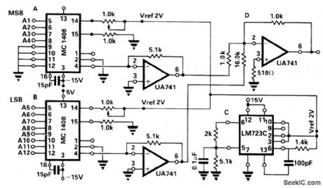
Two MC1408-8-bit D/A converters, A and B in the circuit diagram, are used. The four least significant bits of A are tied to zero. The four most significant bits of the 12-bit data are connected to the remaining four input pins. The eight least significant bits of the 12-bit data are connected to the eight input pins of B. The four most significant bits of the 12-bit data together have a weight of 16 relative to the remaining eight bits. Hence, the output from B is reduced by a factor of 16 and summed with the output from A using the summing op-amp configuration D. Voltage regulator chip, LM7236, is used to provide an accurate reference voltage, 2 V, for the MC1408. The full-scale voltage of the converter is 1/16 x 9.9609 + 1 x (9.375) or 9.9976 V. The step size of the converter is 2.4 mV. (View)
View full Circuit Diagram | Comments | Reading(3115)
ULTRAPRECISION_V_F_CONVERTER
Published:2009/7/1 21:17:00 Author:May
The circuit is capable of better than 0.02% error and 0.003% nonlinearity for a ±20℃ range about room temperature. (View)
View full Circuit Diagram | Comments | Reading(0)
VOLTAGE_TO_FREQUENCY_CONVERTER_1
Published:2009/7/1 21:13:00 Author:May
View full Circuit Diagram | Comments | Reading(841)
VOLTAGE_TO_FREQUENCY_CONVERTER
Published:2009/7/1 21:11:00 Author:May
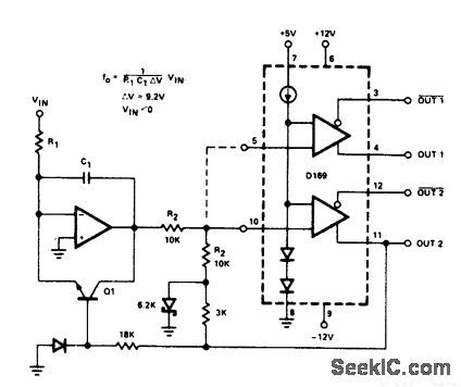
The D169 serves as a level detector and provides complementary outputs. The op amp is used to integrate the input signal VIN with a time constant of R1C1. The input (must be negative) causes a positive ramp at the output of the integrator which is summed with a nega-tive zener voltage. When the ramp is positive enough D169 outputs change state and OUT 2 flips from negative to positive. The output pulse repetition rate f0, is directly proportioned to the negative input voltage VIN. (View)
View full Circuit Diagram | Comments | Reading(0)
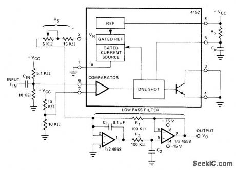
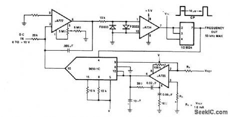
10_Hz_TO_10_kHz_VOLTAGE_FREQUENCY_CONVERTER
Published:2009/7/1 21:09:00 Author:May
View full Circuit Diagram | Comments | Reading(839)
FREQUENCY_TO_VOLTAGE_CONVERTER
Published:2009/7/1 3:52:00 Author:May

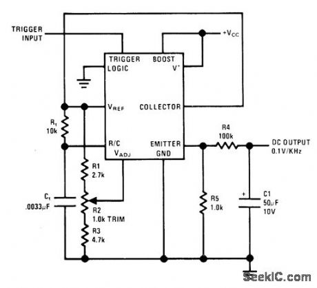
National LM122 timer is used as tachometer by averaging output pulses with simple filter.Pulse width is ad justed with R2 to provideinitialcalibration at 10 kHz. Linearity is about 0.2% foroutput range of 0-1 V. Analog metercan be driven directly by connecting it in series with R5.Supply can range from 4.5 to 40 V.-C. Nelson, Versatile Timer Operates from Microsecondsto Hours, National Semiconductor, Santa Clara, CA, 1973, AN-97, p 10. (View)
View full Circuit Diagram | Comments | Reading(0)
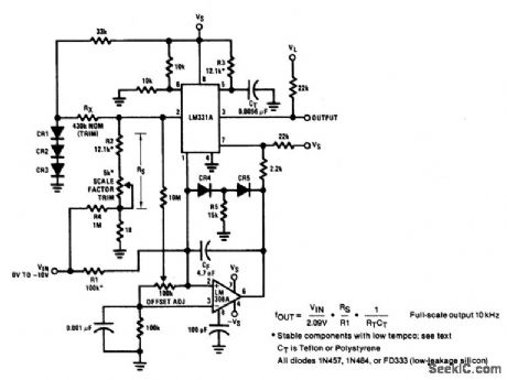
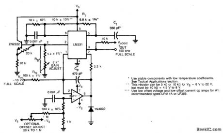
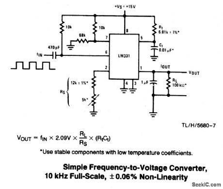
SIMPLE_FREQUENCY_TO_VOLTAGECONVERTER(10_kHz_FULL_SCALE,±0006_NON_LINEARITY)
Published:2009/7/1 3:28:00 Author:May
View full Circuit Diagram | Comments | Reading(848)
FREQUENCY_TO_VOLTAGE_CONVERTER(DIGITAL_FREQUENCY_METER)
Published:2009/7/1 2:43:00 Author:May

Circuit NotesThis circuit converts frequency to voltage by taking the average dc value of the pulses from the 74121 monostable multivibrator. The one shot is triggered by the positive-going ac signal at the input of the 529 comparator.The amplifier acts as a dc filter, and also provides zeroing. The accuracy is 2% over a 5 decade range. The input signal to the comparator should be greater than0.1 volt peak-to-peak, and less than12 volts peak-to-peak for proper operation. (View)
View full Circuit Diagram | Comments | Reading(3447)
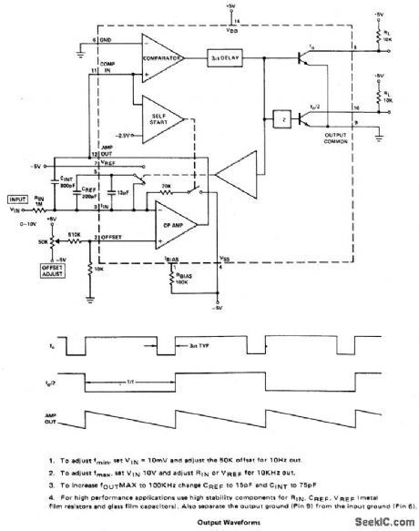
DC_10_kHz_FREQUENCY_VOLTAGE_CONVERTER
Published:2009/7/1 2:39:00 Author:May
Circuit Notes
The converter generates an output vol-tage which is linearly proportional to the input frequency waveform. Each zero crossing at the comparator's input causes a precise amount of change to be dispensed into the op amp's sum-ming junction. This charge in turn flows through the feedback resistor generating voltage pulses at the output of the op amp.Capacitor (CINT) across Rtxt averages these pulses into a dc voltage which is linearly proportional to the input frequency. (View)
View full Circuit Diagram | Comments | Reading(0)
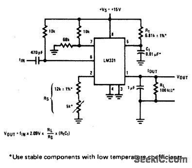
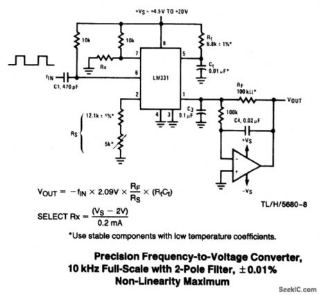
PRECISION_VOLTAGE_TO_FREQUENCY_CONVERTER
Published:2009/7/1 2:05:00 Author:May

In this circuit, integration is performed by using a conventional operational amplifier and feedback capacitor, CF. When the integrator's output crosses the nominal thresh-old level at pin 6 of the LM131, the timing cycle is initiated. The average current fed into the op amp's summing point (pin 2) is i × (1.1 RtCt) × fwhich is perfectly balanced with -VIN/RIN. In this circuit, the voltage offset of the LM131 input comparator does not affect the offset or accuracy of the V-to-F converter as it does in the stand-alone V-to-F converter, nor does the LM131 bias current or offset current. Instead, the offset voltage and offset current of the operational amplifier are the only limits on how small the signal can be accurately converted.
(View)
View full Circuit Diagram | Comments | Reading(1063)
100_MHz_CONVERTER
Published:2009/7/1 2:01:00 Author:May
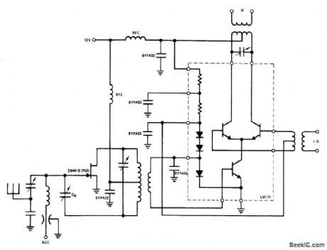
The 2N4416 JFET will provide noise figures of less than 3 dB and power gain of greater than 20 dB. The JFET's outstanding low crossmodulation and low intermodulation distortion provides an ideal characteristic for an input stage. The output feeds into an LM171 used as a balanced mixer. This configuration greatly reduces local oscillator radiation both into the antenna and into the if strip and also reduces rf signal feedthrough. (View)
View full Circuit Diagram | Comments | Reading(1049)
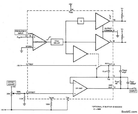
FREQUENCY_TO_VOLTAGE_CONVERTERS
Published:2009/7/1 1:58:00 Author:May
In these applications, a pulse input at fIN is differentiated by a C-R network and the negative-going edge at pin 6 causes the input comparator to trigger the timer circuit.Just as with a V-to-F converter, the average current flowing out of pin 1 is IAVERAGE = i x (1.1 R1C1) x f. In this simple circuit, this current is filtered in the network Rt = 100 k ohm and 1 μF. The ripple will be less than 10 mV peak, but the response will be slow, with a 0.1 second time constant, and settling of 0.7 second to 0.1% accuracy.In the precision circuit,an operatiot amplifier provides a buffered outputand also acts as a 2-pole filter.The ripple will be less than 5 mV peak forall frequenciesabove 1 kHz,and the response time will be much quicker than in Part 1,However,for input frequencies below 200 Hz,this circuit will have worse ripple than the figure。The engineering of the filter time-constants to get adequate response and small enough ripple simply requlres a study of the compromises to be made.Inherently V-to-Fconverter response can be fast, but F-to-Ⅴ response cannot. (View)
View full Circuit Diagram | Comments | Reading(1184)
RMS_TO_DC_CONVERTER
Published:2009/7/1 1:58:00 Author:May
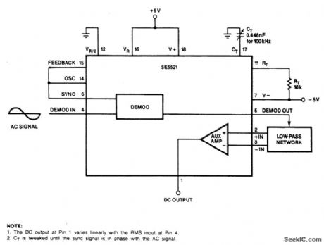
An ac voltmeter may be easily constructed. Simplicity of the circuit and low component count make it particularly attractive. The demodulator output is a full-wave rectified signal from the ac input at Pin 4. The dc component on the rectified signal at Pin 5 varies linearity with the rms input at Pin 4 and thus provides an accurate rms-to-dc conversion at the output of the filter (Pin 1). CT is a variable capacitor that is tweaked until the oscillator signal to the sync input of the demodulator is in phase with the ac signal at Pin 4. (View)
View full Circuit Diagram | Comments | Reading(1287)
| Pages:14/24 1234567891011121314151617181920Under 20 |
Circuit Categories
power supply circuit
Amplifier Circuit
Basic Circuit
LED and Light Circuit
Sensor Circuit
Signal Processing
Electrical Equipment Circuit
Control Circuit
Remote Control Circuit
A/D-D/A Converter Circuit
Audio Circuit
Measuring and Test Circuit
Communication Circuit
Computer-Related Circuit
555 Circuit
Automotive Circuit
Repairing Circuit