
A/D-D/A Converter Circuit
Index 6
High_speed_10_bit_A_D_converter_using_the_μA_722_and_an_ECG915_operational_amplifier
Published:2009/7/20 3:33:00 Author:Jessie
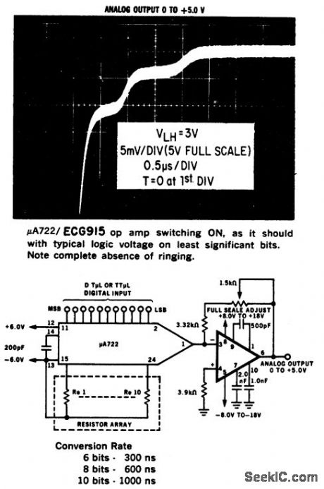
High-speed 10-bit A/D converter using the μA 722 and an ECG915 operational amplifier (courtesy GTE Sylvania Incorporated). (View)
View full Circuit Diagram | Comments | Reading(1200)
4_to_20_mA_converter
Published:2009/7/20 3:31:00 Author:Jessie
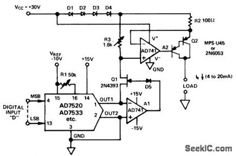
4 to 20 mA converter. The circuit drives a digitally programmed current into a grounded load, RL, according the the relationship IK 4mA (D) (16 mA). With a 10-bit D/A convener such as the AD7520 the circuit provides an output from 4 mA to 20 mA with a resolution of 155/8 μA. The maximum compliance voltage of the load is +25 volts, equivalent to a resistance of 1250 ohms maximum. Higher voltages across the load can be developed if the lower end of RL is returned to a negative voltage, but Q2 must be able to handle the additional breakdown voltage (courtesy Analog Devices, Inc.). (View)
View full Circuit Diagram | Comments | Reading(1675)
D_F_convener_with_complementary_output_frequencies
Published:2009/7/20 3:30:00 Author:Jessie
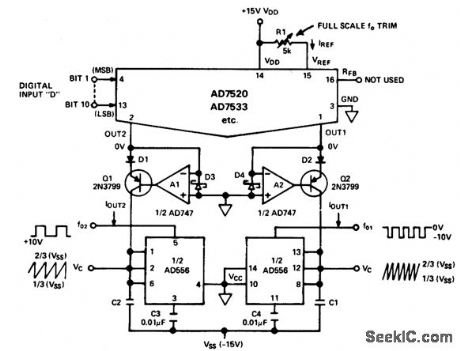
D/F convener with complementary output frequencies. This circuit provides two output frequencies. One output is proportional to the fractional binary equivalent of D, while the other output is proportional to 1 - D. Excellent linearity is obtained from 10 hertz to 10 kilohertz. The 556 timer provides either pulse or sawtooth output waveforms. D1 and D2 are required to protect the emitter-base junctions of Q1 and Q2 during power up. D3 and D4 protect the AD7520 OUT 1 and OUT 2 terminals (courtesy Analog Devices, Inc.). (View)
View full Circuit Diagram | Comments | Reading(1197)
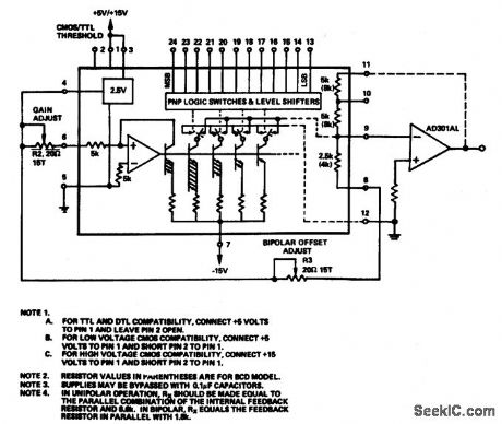
8_bit_D_A_converter_with_bipolar_output
Published:2009/7/20 4:12:00 Author:Jessie
8-bit D/A converter with bipolar output (courtesy Analog Devices, Inc.). (View)
View full Circuit Diagram | Comments | Reading(1032)
D_A_converter_in_bipolar_hookup_using_an_AD563
Published:2009/7/20 4:11:00 Author:Jessie
D/A converter in bipolar hookup using an AD563 (courtesy Analog Devices, Inc.). (View)
View full Circuit Diagram | Comments | Reading(1284)
D_A_converter_in_unipolar_and_bipolar_hookup
Published:2009/7/20 4:10:00 Author:Jessie
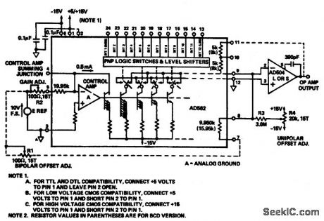
D/A converter in unipolar and bipolar hookup (courtesy Analog Devices, Inc.). (View)
View full Circuit Diagram | Comments | Reading(934)
10_bit_D_A_converter_with_±5_volt_buffered_bipolar_output
Published:2009/7/20 4:09:00 Author:Jessie
10-bit D/A converter with ±5-volt buffered bipolar output (courtesy Analog Devices, Inc.). (View)
View full Circuit Diagram | Comments | Reading(962)
10_bit_D_A_converter_with_unbuffered_±166_volt_bipolar_output
Published:2009/7/20 4:08:00 Author:Jessie
10-bit D/A converter with unbuffered ±1.66-volt bipolar output (courtesy Analog Devices, Inc.). (View)
View full Circuit Diagram | Comments | Reading(872)
10_bit_D_A_converter_with_±10_volt_buffered_output
Published:2009/7/20 4:08:00 Author:Jessie
10-bit D/A converter with ±10-volt buffered output (courtesy Analog Devices, Inc.) (View)
View full Circuit Diagram | Comments | Reading(825)
Power_D_A_converter_using_the_AD7520
Published:2009/7/20 4:07:00 Author:Jessie
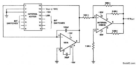
Power D/A converter using the AD7520.The Intersil AD7520 is an 18-pin multiplying DIA converter. This circuit is designed for 8-bit accuracy and 10-bit resolution.The Intersil IH8510 power amplifier(1A continuous output) is driven by the AD7520.A summing amplifier between the AD7520 and IH8510 is used to separate the gain block containing the AD7520 on-chip resistors from the power amplifier stage,whose gain is set only by the external resistors.This approach minimizes drift, otherwise the AD7520 can be directly connected to the IH8510 by using a 25-volt reference for the D/A converter(courtesy Intersil, Inc.). (View)
View full Circuit Diagram | Comments | Reading(1970)
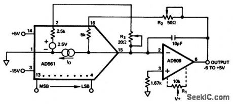
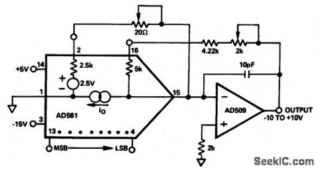
10_bit_DIA_converter_with_an_AD509_op_amp
Published:2009/7/20 4:27:00 Author:Jessie
10-bit DIA converter with an AD509 op amp(courtesy Analog Devices, Inc.). (View)
View full Circuit Diagram | Comments | Reading(930)
D_A_converter_in_unipolar_hookup_using_AD563_12_bit_D_A_converter_chip
Published:2009/7/20 4:25:00 Author:Jessie
D/A converter in unipolar hookup using AD563 12-bit D/A converter chip(courtesy Analog Devices, Inc.). (View)
View full Circuit Diagram | Comments | Reading(883)
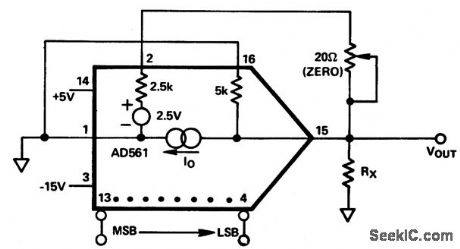
8_bit_D_A_converter_with_voltage_output_and_using_a_fixed_reference
Published:2009/7/20 4:24:00 Author:Jessie

8-bit D/A converter with voltage output and using a fixed reference. For RREF at 1k,2.5k or 5k the minimum value of C should be 15 pF,37 pF or 75 pF respectively(courtesy Analog Devices, Inc.). (View)
View full Circuit Diagram | Comments | Reading(1060)
10_bit_DIA_converter_with_an_AD505_op_amp
Published:2009/7/20 4:23:00 Author:Jessie
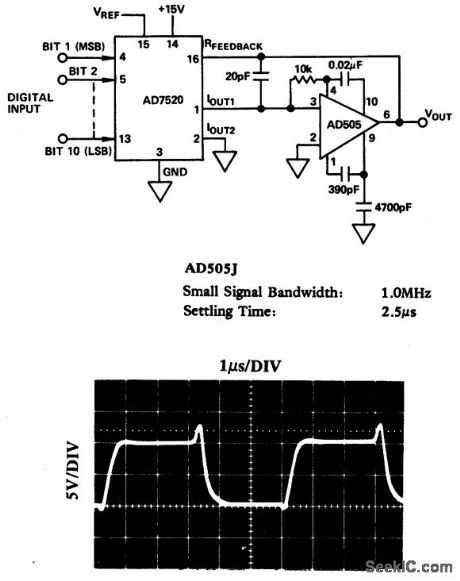
10-bit DIA converter with an AD505 op amp (courtesy Analog Devices, Inc.). (View)
View full Circuit Diagram | Comments | Reading(959)
V_F_converter_with_20_kHz_full_scale_output_offset_to_improve_dynamic_response
Published:2009/7/20 4:23:00 Author:Jessie
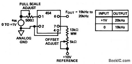
V/F converter with 20 kHz full scale output offset to improve dynamic response (courtesy Analog Devices, Inc.). (View)
View full Circuit Diagram | Comments | Reading(850)
V_F_converter_using_a_flip-flop_to_obtain_a_square_wave_output
Published:2009/7/20 4:22:00 Author:Jessie
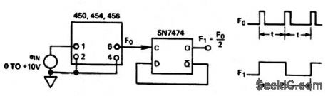
V/F converter using a flip-flop to obtain a square wave output.The full scale output for the 450 and 456 is 10 kHz and 20 kHz for the 454(courtesy Analog Devices, Inc.). (View)
View full Circuit Diagram | Comments | Reading(854)
V_F_converter_offset_for_bipolar_operation_
Published:2009/7/20 4:21:00 Author:Jessie
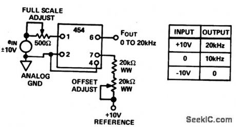
V/F converter offset for bipolar operation (courtesy Analog Devices, Inc.). (View)
View full Circuit Diagram | Comments | Reading(800)
12_bit_successive_approximation_A_D_converter_for_bipolar__10_volt_to__10_volt_input_range_with_buffer_followerThe_A_D_chip_is_the_AD572
Published:2009/7/20 4:21:00 Author:Jessie
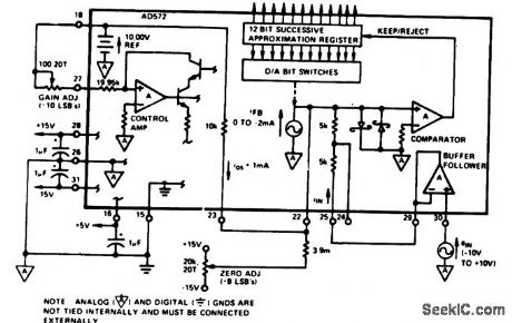
12-bit successive approximation A/D converter for bipolar -10 volt to+10 volt input range with buffer follower,The A/D chip is the AD572(courtesy Analog Devices, Inc.). (View)
View full Circuit Diagram | Comments | Reading(932)
10_bit_D_A_converter_with_an_AD741_op_amp
Published:2009/7/20 4:18:00 Author:Jessie
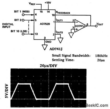
10-bit D/A converter with an AD741 op amp (courtesy Analog Devices, Inc.). (View)
View full Circuit Diagram | Comments | Reading(1028)
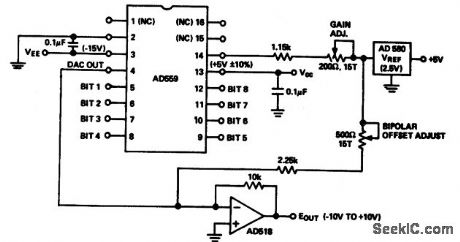
10_bit_DIA_converter_with_an_AD518_op_amp
Published:2009/7/20 4:17:00 Author:Jessie
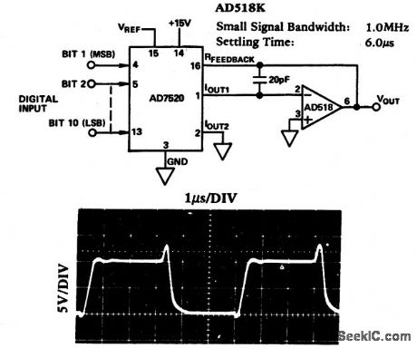
10-bit DIA converter with an AD518 op amp (courtesy Analog Devices, Inc.). (View)
View full Circuit Diagram | Comments | Reading(1103)
| Pages:6/24 1234567891011121314151617181920Under 20 |
Circuit Categories
power supply circuit
Amplifier Circuit
Basic Circuit
LED and Light Circuit
Sensor Circuit
Signal Processing
Electrical Equipment Circuit
Control Circuit
Remote Control Circuit
A/D-D/A Converter Circuit
Audio Circuit
Measuring and Test Circuit
Communication Circuit
Computer-Related Circuit
555 Circuit
Automotive Circuit
Repairing Circuit