
A/D-D/A Converter Circuit
Index 17
_5_V_TO__7_V
Published:2009/6/30 2:24:00 Author:May
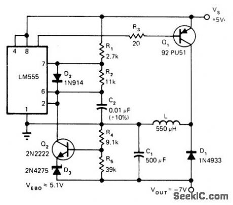
Uses LM555 timer as variable-duty-cycle pulse generator controlling transistor switchQ1 which in turn drivesflyback circuit.Regulator Q2-D3-R4-R5 varies duty cycle according to load, and flyback circuit L-D1-C1 develops negative output voltage. When Q1 is on, current flows through L to ground. When Q1 turns off, polarity across L reverses, diode becomes forward-biased, and negative voltage appears across C1 and load. When Q1 turns on again, voltage across L reverses for start of new cycle. Circuit eliminates separate transformer supply for negative supply of microprocessor. Efficiency is about 60%, load regulation 1.3%, and supply rejection 30 dB. Article gives design equations.—P. Brown, Jr., Converter Generates Negative μP Bias Voltage from +5V, EDN Magazine, Aug.5, 1977, p 42, 44, and 46. (View)
View full Circuit Diagram | Comments | Reading(1599)
_15_V_FROM__15_V
Published:2009/6/30 2:22:00 Author:May

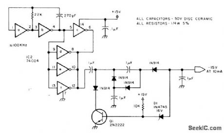
First two sections, of 74C04 hex inverter form 100-kHz oscillitor, with other sections connected to provide inversion of standard microprocessor source voltage as required for some interfaces and some DA converters.Shunt regulator formed by D1 and Q1 maintains output vottage relatively constant.Changing zener D1 to 13 V makes output -12 V.—S. Ciarcia, Build a 5 W DC to DC Converter, BYTE, Oct. 1978, p 22, 24, 26, 28, and 30-31. (View)
View full Circuit Diagram | Comments | Reading(1292)
280_V_T0_600_V
Published:2009/6/30 2:21:00 Author:May
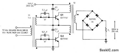
Cascode push-pull transistor switch conversion circuit uses low-voltage transistors and provides automatic equalization of transistor storage time. Drive-signal input to cascode push-pull switch is symmetrical 50-kHz 15 V P-P square wavefrom 50-ohm source. Q1 and Q2 each see only haff of DC source voltage because C1 and C2, in series across 280-V input, charge to 140 V each. Circuit is adaptable to wide range of output voltages and currents because identical units can be connected in series or parallel to obtain desired rating.—L. G.Wright and W. E. Milberger, HV Building Block Uses Series Transistor Switches, EDN Magazine, Feb. 15, 1971, p 39-40. (View)
View full Circuit Diagram | Comments | Reading(1052)
5_V_TO_400_V
Published:2009/6/30 2:16:00 Author:May
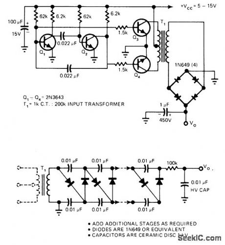
Astable MVBR operating at 2.174 kHz for values shown drives push-pull transistor pair feeding primary of audio input transformer T1. Secondary voltage is rectified by diode bridge to provide DC output voltage ranging from 100 to 400 V depending on load resistance and exact value of supply voltage VCC.Bridge rectifier can be replaced by 40-stage multiplier as shown in lower diagram, to give 10-kVDC output.—A. M. Hudor, Jr., Power Converter Uses Low-Cost Audio Transformer, EDN Magazine, April 20, 1977, p 139. (View)
View full Circuit Diagram | Comments | Reading(1347)
_12V_TO__8_V
Published:2009/6/30 2:14:00 Author:May
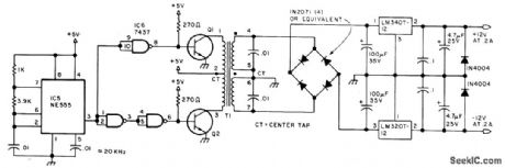
NE555 timer connected as 20-kHz oscillator drives pair of D44H4 transistors through 7437 quad two-input NAND buffer to produce full 200 mA of regulated output for each polarity. Circuit uses push-pull inverter technique to generate AC for driving transformer constructed by rewinding 88-mH toroid to have 40 turns No, 20 center-tapped for primary and 350 turns No. 26 center-tapped for secondary.—S, Ciarcia, Build a 5 W DC to DC Converter, BYTE, Oct. 1978, p 22, 24 26, 28, and 30-31. (View)
View full Circuit Diagram | Comments | Reading(2834)
6_V_TO_±15_V
Published:2009/6/30 2:12:00 Author:May
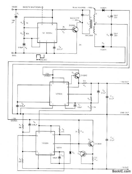
Combination of 555 timer and two NE550 voltage regulators provides voltage mu Itiplication along with regulation of independent DC outputs. Selected oscillator frequency of 17 kHz optimizes performance of transformer. Can be used to power opamps from either TTL supplies or 6-V batteries. Line and load regulationare 0.1 %, while power efficiency at full load of 100 mA is better than 75%.—R.Solomon and R. Broadway, DC-to-DC Converter Uses IC Timer, EDN Magazine, Sept. 5, 1973, p 87, 89, and 91. (View)
View full Circuit Diagram | Comments | Reading(1446)
_6V_TO±15V
Published:2009/6/30 2:03:00 Author:May
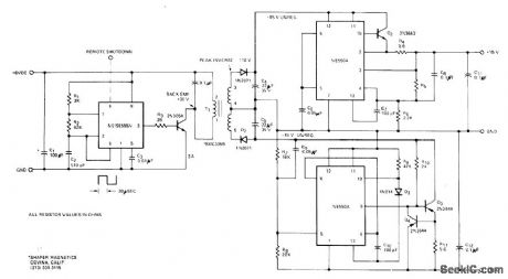
Combination of 555 timer andtwo NE550A Precision adjustable regulators gives 0.1% line and load regulation,Timer operates as osdllator driving step-up transformer which feeds full-wave rectffier.— Signetics Analog Data Manual, signetics,Sunnyvale,CA,1977,p 726-727. (View)
View full Circuit Diagram | Comments | Reading(990)
2_V_TO_2O_AND_15O_V
Published:2009/6/30 2:02:00 Author:May
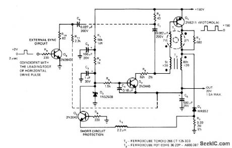
Use of 7-turn toroidal transformer in self-excited dnging-choke blocking-oscillator circuit improves efficiency of converter circuit by providing fast switching time. Circuit is practical only when input and output voltages differ signfficantly. Blocking oscillator is formed by Q1, T2, C1, R2, and base-bias network R6-Q2. Q4 makes possible external synchronization, permitting use in television systems for triggering regulator with leading edge of horizontal drive pulse. This ensures completion of cycle within blanking interval.—N. Tkacenko, Transformer Increases DC-DC Converter Efficiency to 80%, EDN Magazine, May 5, 1976, p 110 and 112. (View)
View full Circuit Diagram | Comments | Reading(1381)
1_12_V_TO__12_V
Published:2009/6/30 2:00:00 Author:May
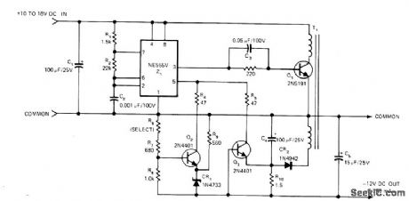
Transforms unregulated +12 VDC to current-Iimited regulated -12 VDC. Front end of 555 is connected in astable configuration, with R2 selected to give about 25 kHz at pin 3. Control of modulation input to pin 5 gives voltage regulation and current limiting. Circuit tolerates continuous operation under short-circuit conditions. With 10-V nominal output, line regulation is within 0.05% for input and output voltage ranges of 0.3 to 10 V. Load regulation is 0.2% for loads from 10 μA to 10mA when load impedance is 10 ohms,—R.Dow,Build a Short-Circuit-Proof +12V Inverter,with One IC,EDN Magazine,Sept 5,1977,p 177-178 (View)
View full Circuit Diagram | Comments | Reading(985)
_12_V_TO__12_V
Published:2009/6/30 1:59:00 Author:May
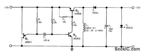
Transformerless inverting DC-to-DC converter has above 55% effciency and can withstand output shorts lasting up to several minutes. UJT Q1 and base-emitter diode of transistor Q2 from free-running MVBR whose 25-kHz output is amplified by Q2 to drive switching-mode converter Q3-L1-D1-C2. Zener D2 regulates output for variations in input voltage or output loads up to 40 mA.—G. Bank, Transformerless Converter Supplies Inverted Output, EDN|EEE Magazine, July 1, 1971, p 48. (View)
View full Circuit Diagram | Comments | Reading(1063)
4_BIT_CLOCKLESS
Published:2009/6/30 1:56:00 Author:May

Simple and low-cost arrangement of seven CA3130 opamps gives conversion times fast enough for tracking sinewave signals well up into audio range, Even with relatively slow 741 opamps, signals up to 300 Hz were easily tracked. Additional bits are easily cascaded.—B. P. Vandenberg, Tracking-Type A/D Requires No Clock Oscillator, EDN Magazine, Jan. 20, 1977, p 92 and 94. (View)
View full Circuit Diagram | Comments | Reading(1175)
COMPRESSING_A_D_CONVERSION
Published:2009/6/30 1:50:00 Author:May
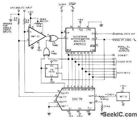
Step size increases as output changes from zero scale to full scale, in contrast to conventional linear converter in which step size is constant percentage of full scale. Uses Precision MonolithIcs DAC-76 D/A converter in combination with CMP-01 comparator, any standard EXCLUSIVE-OR gate, and successive-approximation register for conversion logic. Encoding sequence begins with sign-bit comparison and decision. Bits are con verted with successive-removal technique, starting with decision at code 011 1111 and turning off bits sequentially until all decisions have been made. Conversion is completed in nine clock cycles.— COMDAC Companding D/A Converter, Precision MonolithIcs, Santa Clara, CA, 1977, DAC-76, p 12. (View)
View full Circuit Diagram | Comments | Reading(1237)
HIGH_SPEED_SUCCESSIVE_APPROXIMATION
Published:2009/6/30 1:46:00 Author:May

Total converslon time for 8-bit system is about 4.5 μs,clock rate is up to 2 MHz. Serial output is used for transmission to one or more other location. —T. Henry, Successive Approximation A/D Conversion, Motorola, Phoenix, AZ, 1974, AN-716, p 5. (View)
View full Circuit Diagram | Comments | Reading(1437)
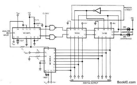
FOUR_CHANNEL_INPUT_MULTlPLEXING
Published:2009/6/30 1:40:00 Author:May
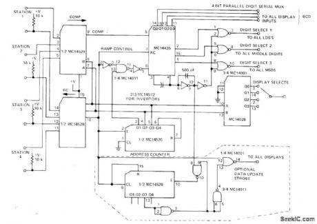
Conversion process is divided between central station and remote locations having analog sensors. Each station transmits two noise-immune low-frequency digital signals under control of central multiplexor. System is much more economical than having separate A/D converter at each sensor. Can be extended to 32 channels. Multiplexing is performed under control of clock in Motorola MC14435, operating between 100 kHz and 1 MHz. At 500 kHz, each conversion takes about 15 ms.—S. Kelley, Analog Data Acquisition Network for Digital Processino Using the MC1405-MC14435 A/D System, Motorola, Phoenix, AZ, 1975, EB-58. (View)
View full Circuit Diagram | Comments | Reading(1235)
DIFFERENTIAL_CONVERSION
Published:2009/6/30 1:34:00 Author:May
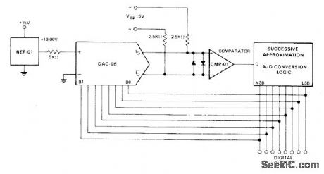
Uses high current output capability of Precision Monolithics DAC-08 D/A converter and high common-mode voltage rejection of CMP-01 comparator to give differential-input ADC without input signal conditioning. Successive-approximation conversion logic is obtained with REF.01 +10 V reference and 2502-type successive-approximat ion register, driven by DAC and comparator. Analog input is converted in less than 2 μs. Differential input range is 5 V. Diodes are 1N4148.—J. Schoeff and D. Soderquist, Differential and Multiplying Digital to Analog Converter Applications, Precision MonolithIcs, Santa Clara, CA, 1976, AN-19, p 5. (View)
View full Circuit Diagram | Comments | Reading(1721)
TRACKING_A_D_CONVERTER
Published:2009/6/30 1:33:00 Author:May
Addition of one gate to tracking or servorype A/D converter, as shown in dashed box, overcomes instability problems otherwise occurring when input voltages are less than zero or greater than full scale. With 8-bit converter shown, count of 11111111 when counting up makes carry output and load inputs go low, holding counter in this state so subsequent up clocks are ignored. When count is all 0s, borrow output goes low and clear input goes high, so counter isfree to countup only.—A. Helfrick, Tracking A/D Converters Need Another Look, EDN Magazine, June 20, 1975, p 118 and 120. (View)
View full Circuit Diagram | Comments | Reading(1563)
Current_to_voltage_converter
Published:2009/7/24 21:21:00 Author:Jessie
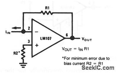
The output of this circuit is directly proportional to the input current, multiplied by the value of R1. (View)
View full Circuit Diagram | Comments | Reading(0)
Precision_ac_to_dc_converter
Published:2009/7/24 22:59:00 Author:Jessie
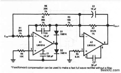
This circuit converts the half-wave rectifier or Fig. 10-39 to a full-wave rectifier. The conversion accuracy is better than 1% to above 100 kHz, with less than 1% ripple at 20 Hz. Using the values shown, the output is calibrated to read the rms value of a sine-wave input. (View)
View full Circuit Diagram | Comments | Reading(3392)
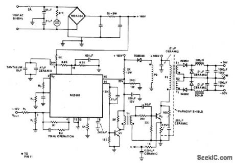
±50_V_FEED_FORWARD_SWITCH_MODE_CONVERTER
Published:2009/6/28 21:23:00 Author:May
View full Circuit Diagram | Comments | Reading(1318)
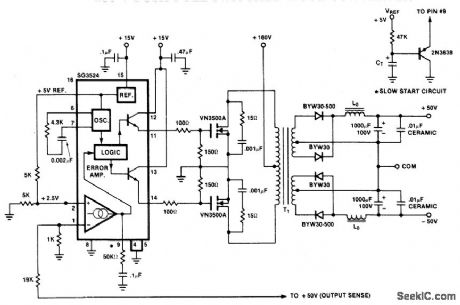
±50_V_PUSH_PULL_SWITCHED_MODE_CONVERTER
Published:2009/6/28 21:21:00 Author:May
View full Circuit Diagram | Comments | Reading(2452)
| Pages:17/24 1234567891011121314151617181920Under 20 |
Circuit Categories
power supply circuit
Amplifier Circuit
Basic Circuit
LED and Light Circuit
Sensor Circuit
Signal Processing
Electrical Equipment Circuit
Control Circuit
Remote Control Circuit
A/D-D/A Converter Circuit
Audio Circuit
Measuring and Test Circuit
Communication Circuit
Computer-Related Circuit
555 Circuit
Automotive Circuit
Repairing Circuit