
Index 86
FAX_MATE
Published:2009/6/16 2:03:00 Author:May

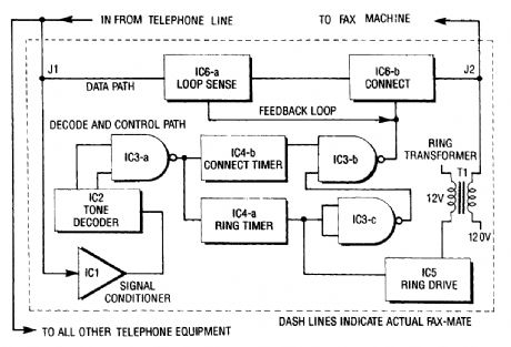
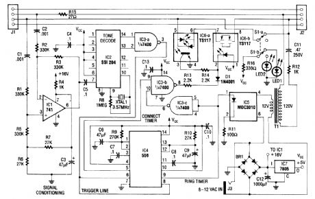
The fax mate separates the fax machine from the phone line, rings the fax machine on com-mand, connects equipment to incoming lines, and senses the end of the message. When a touch tone pound signal (#) is detected, it actuates a ring greater and driver for the fax machine (the # signal is not used in ordinary dialing). The connect signal is inhibited for this time (ring cycle).1C46 runs for 15 s and drives part of the connect IC. Then the fax or modem has fired up and is sending out a handshake tone. IC6 connects the equipment for initial hookup and keeps the connect section powered. When the fax machine hangs up, the loop current detector turns off, and resets the system. (View)
View full Circuit Diagram | Comments | Reading(2265)
CD_IGNITION_SYSTEM_FOR_AUTOS
Published:2009/6/16 Author:May
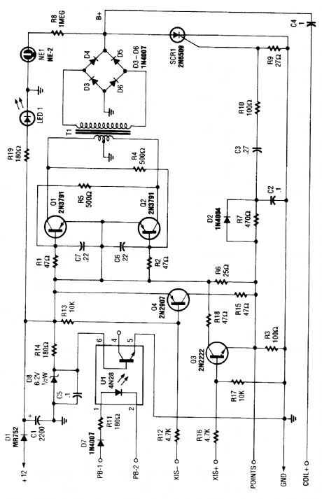
At the heart of the CD4-MX is an astable multivibrator, built around Q1 and Q2, that feeds step-up transformer T1. The out-put of T1 is rectified by D3 to D6 and used to charge capacitor C4. When the points colse, a small voltage is fed to the gate of SCR1, causing it to fire, dumping the charge of C4 to the vehicle's ignition coil. The circuit also contains optional subciruits to accommodate different types of auto ignitions.X15 + and X15 - are alternative trigger configurations for nonponit breaker ignition systems. R6 is not used for these systems and must be removed. Optocoupler U1 can be used (pin 4) in conjunction with X15 - or X15 + depending on polarity of sensor. Note that 60 to 70 kV is available from this system, so observe suitable safety precautions. (View)
View full Circuit Diagram | Comments | Reading(994)
AGC_SYSTEM_FOR_AUDIO_SIGNALS
Published:2009/6/15 23:32:00 Author:May
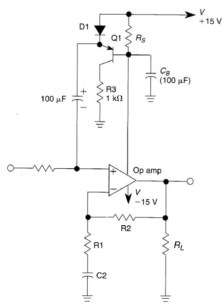
This circuit is an AGC system for audio-fre-quency signals. AGC systems usually consist of three parts: an amplifier, rectifier, and controlled impedance. In this circuit the functions of an ampltfier and a rectifier are performed by a single op amp. This makes the system simple and cheap.The rectifier is made with the output push-pull cascade of the op amp and RS, RL, and CB. The transistor Q1 and D1 are used as a voltage-controlled resistance (Z). The input signal is (Z + R1)/Z times, diminished by the voltage divider and 1 + R2/R1 times, amplified by the op amp. C2 eliminates influence of dc bias voltage. R3 protects Q1 and D1 from excessive current. (View)
View full Circuit Diagram | Comments | Reading(2301)
AUDIO_BOOSTER
Published:2009/6/15 23:09:00 Author:May
This circuit has a maximurn gain of about 22 dB (voltage gain), and it can be used for miscel-laneous audio circuits. (View)
View full Circuit Diagram | Comments | Reading(1677)
AUDIO_COMPRESSOR
Published:2009/6/15 23:02:00 Author:May
This compressor will compress a 25-mV p-p to 20-V p-p audio output to input levels remaining between 1.5Vp-p to 3.5 V p-p, and has a frequency response of 7 Hz to 67 kHz. It is suitable for audio and communications applications. (View)
View full Circuit Diagram | Comments | Reading(4)
455_kHz_FM_DEMODULATOR
Published:2009/6/15 22:57:00 Author:May
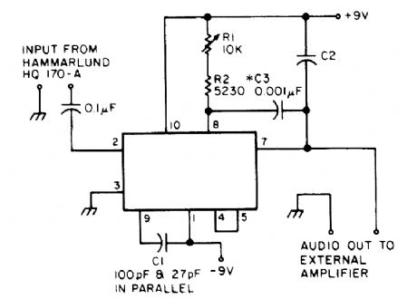
Free-running frequency of VCO:fos=1.2/4(R1)(C1) lock range f1=±8fos/VCC capture rang fc=±1/2π where r=(3.6×10³)(C2)
Useful for NBFM reception on older shortwave receivers lacking this capability,this circuit uses a PLL IC,an N565N,to achieve this.It was originally used with an old Hammarlund HQ-170 receiver, for both 6-and 10-m FM reception. (View)
View full Circuit Diagram | Comments | Reading(1000)
AUDIO_LINE_DRIVER
Published:2009/6/15 22:50:00 Author:May
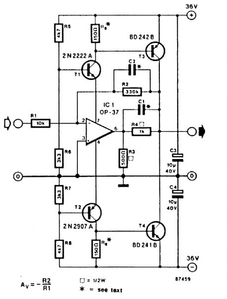
This line driver can drive low-impedance lines with up to 70 V p-p max. IC1 is a low-noise op amp suitable for ±15-V operation. T1 and T2 are regulators for the power supply for IC1. T3 and T4 form a complementary power output stage. Frequency response is flat up to 100 kHz. (View)
View full Circuit Diagram | Comments | Reading(1093)
FM_DEMODULATOR
Published:2009/6/15 22:23:00 Author:May
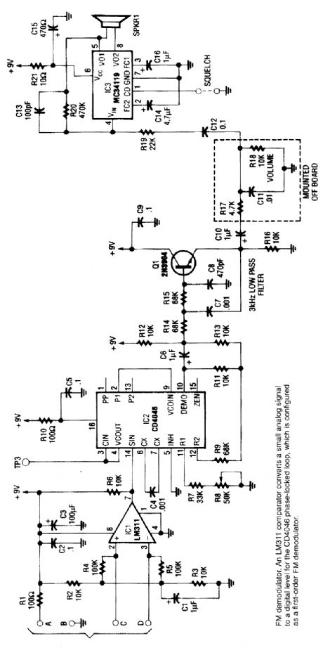
An LM311 comparator converts a small analog signal to a digital level for the DC4046 phase-locked loop, which is config-ured as a first-order FM demodulator. This demodulator works with a 50-kHz FM modulated input signal. It has applications in FM light beam receivers or in remote control applications. Pin 1 of IC3 can be used to squelch the receiver if it is lifted from ground if not desired, leave it grounded. (View)
View full Circuit Diagram | Comments | Reading(3)
INRUSH_CURRENT_LIMITER
Published:2009/6/15 22:02:00 Author:May
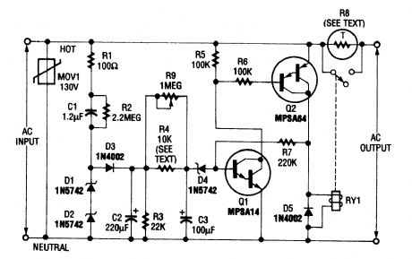
Q1 is an npn Darlington and Q2 is a pnp Darlington. MOV1 is a metal-oxide varistor and R8 is an NTC thermistor for limiting inrush current.This circuit limits ac line current to a load. When a predetermined interval has passed, RY1 shorts out thermistor or resistance RB. R4 can be 150 kΩ if R9 is not used. If power is removed, the circuit is ready for immediate restart. (View)
View full Circuit Diagram | Comments | Reading(4034)
LOW_POWER_ANTENNA_TUNER
Published:2009/6/15 21:15:00 Author:May
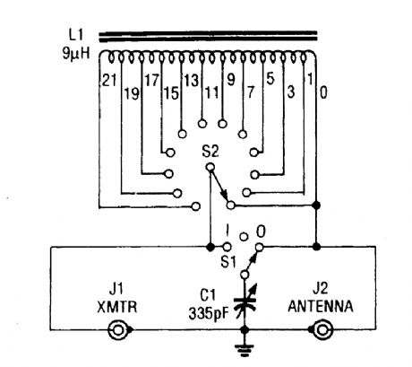
This antenna tuner is suitable for use with low-power (less than 5 W) transmitters or SW re-ceivers. 52 selects inductance and 52 connects the 365-pF capacitor to either the transmitter or the side of the inductor. The tiny tuner is comprised of a tapped inductor (L1) and a variable capacitor (C1), which is connected to the induc-tor through a center-off SPDT switch (S1). That switch arrangement permits the capacitor to be connected to either the input or the output of the circuit. (View)
View full Circuit Diagram | Comments | Reading(1736)
SIMPLE_BALUN
Published:2009/6/15 21:01:00 Author:May
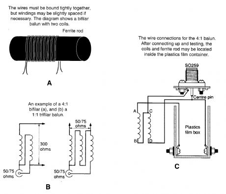
An old fettite rod from a junked broadcast receiver can be used to construct an antenna balun, as shown. (View)
View full Circuit Diagram | Comments | Reading(804)
VLF_VHF_WIDEBAND_LOW_NOISE_ACTIVE_ANTENNA
Published:2009/6/15 20:55:00 Author:May
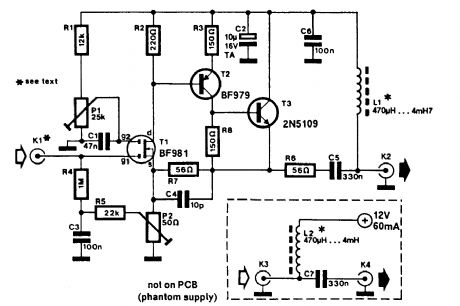
A 30- to 50-cm whip antenna provides reception from 10 kHz to over 220 MHz. T1, a dual-gate MOSFET, provides low noise, high-input impedance, and high gain.The circuit is powered via the coaxial cable used to connect the antenna to a receiver. (View)
View full Circuit Diagram | Comments | Reading(2442)
10_MHz_FREQUENCY_COUNTER
Published:2009/6/15 20:51:00 Author:May
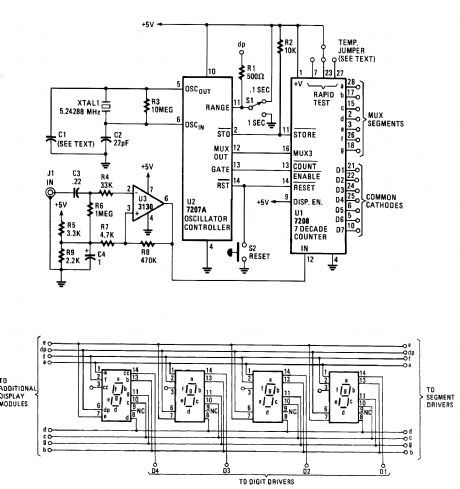
The circuit consists of an ICM7208 seven-decade counter (U1), an ICM7207A oscillator controller (U2), and a CA3130 biFET op amp (U3). Integrated circuit UI counts input signals, decodes them to 7-segment format, and outputs signals that are used to drive a 7-digit display. Integrated cir-cuit U2 provides the timing for UI, while U3 conditions the input signal to provide a suitable wave-form for input to UI. The 5.24288-MHz crystal frequency is divided by U2 to produce a 1280-Hz multiplexing signal at pin 12 of U2. That signal is input to UI at pin 16 and is used to scan the display digits in sequence. The cathodes of each digit are taken to ground several times each second, acti-vating any segments of the digits whose anodes are high as the result of decoding by UI. The crystal frequency is further divided to produce a short store pulse at pin 2 of U2, followed (after about 0.4 ms) by a short reset pulse at pin 14 of U2. The frequency of the pulses is determined by the state of U2 pin 11.When pin 11 of U2 is taken to ground through S1, the pulses occur every 2 seconds and cause U2 pin to go high for one second, which prevents additional input signals from entering UI. That causes the count latched in UI's internal counters to be transferred to the display.Integrated circuit U2 pin 13 then goes low for one second, allowing a new count to be entered into the seven decade counters of UI. That cycle is repeated, continuously updating the display every two seconds.When U2 pin 11 is taken to the positive supply rail (+5 V), the store and reset pulses occur at 0.2-s intervals, resulting in a 0.1-s count-period. Ten input pulses must be counted in order for a 1 to appear on the first digit, Dl, so that the frequency being measured is obviously 10 times larger than the frequency that is shown on the display. In that mode, the decimal points are driven by M and visually indicate that the 0.1-s count period is being used.The display must have at least seven 7-segment common-cathode multiplexed LED digits. Any common-cathode seven-segment display can be used; no particular display is specified. (View)
View full Circuit Diagram | Comments | Reading(3075)
STROBE_ALERT_SYSTEM
Published:2009/6/14 21:47:00 Author:May
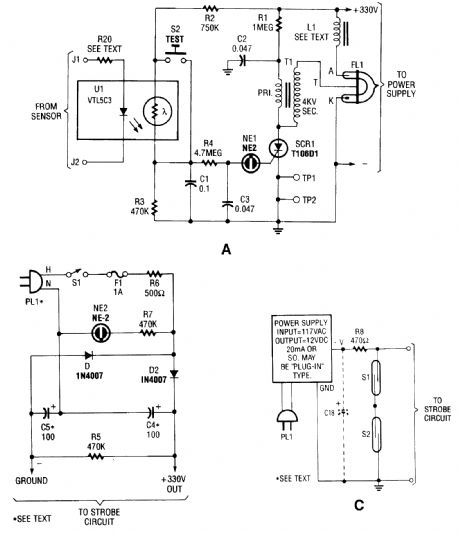
The circuit is activated by an LED/photoresistor isolator (U1), which is a combination of a light-dependent resistor (LDR) and an LED in a single package. That device was chosen because of its high isolation (2000 V) characteristic, which is necessary because the strobe part of the circuit is di-rectly connected to the ac line.The voltage divider is formed by R2, UI's internal resistance, and R3. When UI's internal LED is off, UI's internal LDR has a very high resistance-on the order of 10 MO. The voltage applied to NE1 is considerably below its ignition voltage of approximately 90 Vdc.The optoisolator's internal LED is activated by a dc signal supplying 20 mA. The external sen-sor(s) that supply the signal are connected to the strobe part of the circuit at J1 and J2.When the internal LED lights, the LDR's resistance decreases to around 5 kΩ. Under that con-dition, about 125 Vdc is applied across C1, R4, and C2. The neon lamp periodically fires and extin-guishes as capacitor C3 charges through R4, and discharges via NE1 and the SCR gate.Rests!or R4 restricts the current input to C3, and thereby controls the firing rate of NEl-about three times per second. The discharge through NE1 is applied to the gate of SCR1.SCR1, a sensitive-gate unit, snaps on immediately when NE1 conducts, which completes the ground circuit for transformer T1 (a 4-kV trigger transformer). As SCR1 toggles on and off in time with the firing of NE1, capacitor CZ (connected in parallel with T1's primary) charges via RI, and then discharges very rapidly through T1's primary winding. A voltage pulse is applied to the trigger input of ELI, a Xenon flash lamp.It is important to remember that the circuit is connected directly to the ac line. Resistor R6 is in-cluded to limit the amount of line current available to the circuit. The value of R6 can be decreased if you intend to modify the circuit for more flash power.Warning: Even though the circuit is fuse-protected, it can still be dangerous if handled care-lessly. (View)
View full Circuit Diagram | Comments | Reading(1838)
DOOR_MINDER
Published:2009/6/14 21:45:00 Author:Celina
This circuit monitors a door to detmrmine if it has been left open.After 24 seconds, the alarm sounds.S1 is a magnetic sensor. The alarm is an electronic chime sound that is struck once per second. (View)
View full Circuit Diagram | Comments | Reading(1120)
Digital photoelectric counter(CD4518、CD4543)
Published:2011/7/14 22:39:00 Author:zj | Keyword: Digital, photoelectric counter

The digital electronic counter has intuitive and accurate counting features. It is currently used in a variety industries. The digital electronic counter hasmany counting trigger mode. It is decided bythe actual conditions of use and environment.It can use a mechanical contact type trigger mode, or use electronic sensor's non-contact trigger.A photoelectric sensor is one of them. It is a non-contact electronic sensor.
(View)
View full Circuit Diagram | Comments | Reading(3645)
Digital power factor meter composed of ICL7107
Published:2011/7/18 22:48:00 Author:zj | Keyword: Digital, power factor meter
View full Circuit Diagram | Comments | Reading(6768)
The oscillation circuit with automatic gain control (AGC)
Published:2011/7/17 22:06:00 Author:zj | Keyword: oscillation circuit, automatic gain control
Thediagram is the oscillation circuit with automatic gain control ( AGC). In the circuit, A1 ~ A3 is circuits whichchangeAC signal from the pickup output into a DC signal. The DC signal changes can be used as a comparator A4 input signal, which is then compared with a reference voltage. It does the oscillator output amplitude modulation. Due to the A3 output DC signal fluctuation components, it will affect the normal work of the comparator A4.
(View)
View full Circuit Diagram | Comments | Reading(1413)
LA4275 Circuit
Published:2011/7/26 4:52:00 Author:Robert | Keyword: Circuit
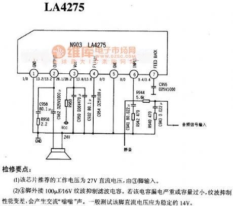
Overhauling notes.
(1)This chip's recommended working voltage is 27V DC voltage on pin 3 for input.
(2)The pin 4 is connected to a external 100uF/16V ripple suppression filter capacitor. If the capacitor has the cases of serious electric leakage or too low capacity, the ripple suppression performance would become bad and this would cause the alternating Weng Weng sound. In general test this pin's DC voltage should be stable 14V. (View)
View full Circuit Diagram | Comments | Reading(1645)
LA4225 Circuit
Published:2011/7/26 2:09:00 Author:Robert | Keyword: Circuit
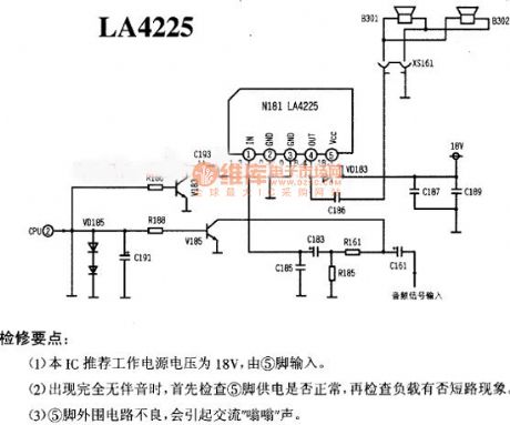
Overhauling notes:
(1)This IC's recommended working power voltage is 18V on pin 5 for input.
(2)If there is fully no accompanying sound, it should firstly check if the pin 5's power supply is normal and then check the if the loading have the short circuit.
(3)If the pin 5's external circuit is not good, it would cause the alternating Weng, Weng sound. (View)
View full Circuit Diagram | Comments | Reading(9140)
| Pages:86/126 At 2081828384858687888990919293949596979899100Under 20 |
Circuit Categories
power supply circuit
Amplifier Circuit
Basic Circuit
LED and Light Circuit
Sensor Circuit
Signal Processing
Electrical Equipment Circuit
Control Circuit
Remote Control Circuit
A/D-D/A Converter Circuit
Audio Circuit
Measuring and Test Circuit
Communication Circuit
Computer-Related Circuit
555 Circuit
Automotive Circuit
Repairing Circuit