
Index 84
PHONE_IN_USE_INDICATOR
Published:2009/6/22 22:18:00 Author:May
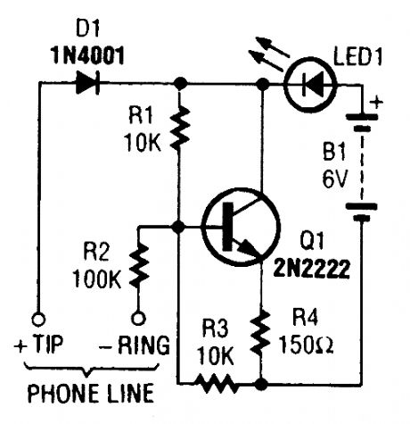
This phone-in-use indicator also indicates the presence of a ring signal. Just the thing for the hearing impaired. (View)
View full Circuit Diagram | Comments | Reading(0)
TELEPHONE_RING_CONVERTER
Published:2009/6/22 22:17:00 Author:May
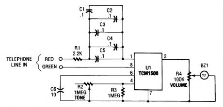
The circuit is based on the TCM1506 ring detector/driver integrated circuit. It is a monolithic IC specifically designed to replace the telephone's mechanical bell. The chip is powered and activated by the telephone-line ring, which can vary from 40 to 150 V rms at a frequency of from 15 to 68 Hz. No other source of power is required. Again, referring to the figure shown, C1 through C5 are placed in parallel to form a 0.5-μF capacitor that conducts the ac ring voltage to pin 1 of the TCM1506, but blocks any dc component. Of course, those capacitors can be replaced by a single 0.47- to 0.5-μF capacitor provided that it has at least a 400-WVdc rating. Resistor R1 is in series with the capacitor network and is used to dissipate power from any high-voltage transient that might appear across the line. The diluted ac voltage that reaches pin 1 on U1 powers the chip.Capacitor C6 is used to prevent bell tapping. That is an annoying ringing of the bell that occurs when a phone on the same line is used to dial an outgoing call. The capacitor prevents the short dial pulses from triggering the ring detector, but still allows the much longer ring signal to activate it.Potentiometer R2 is used to vary the tone of the ring signal from below 100 Hz to over 15 kHz. Potentiorneter R4 is the volume control; adjusting that potentiometer to its lowest resistance will mute the piezo element (BZl). When a ring signal is present on the phone-line, it powers U1. The IC then generates a tone (with a frequency that is determined by R2 and an amplitude set by R4) that is reproduced by BZ1. (View)
View full Circuit Diagram | Comments | Reading(1224)
AUTOMATIC_TELEPHONE_CALL_RECORDING_CIRCUIT
Published:2009/6/22 22:11:00 Author:May
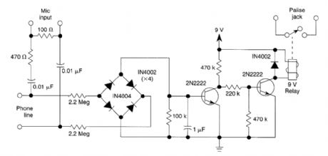
The dc voltage present on a telephone line is usually around 45 to 50 V on-hook and 6 V off-hook. This circuit uses this drop in voltage to activate a relay. The relay controls a cassette tape recorder. Audio is taken off through a network to the microphone input of the cassette. (View)
View full Circuit Diagram | Comments | Reading(1774)
VIDEO_PREAMP
Published:2009/6/19 5:04:00 Author:May
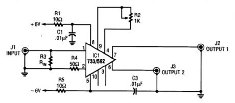
An NE592 or LM733 is used as a general-purpose video amplifier in this schematic. J2 and J3 provide two anti-phase outputs. R2 is a gain control. The bandwidth is about 100 MHz. (View)
View full Circuit Diagram | Comments | Reading(4)
VIDEO_SELECTOR
Published:2009/6/19 5:00:00 Author:May
This circuit selects one of two channels with a logic signal. The unused channel is shorted out, which minimizes crosstalk. The bandwidth at -3 dB is about 8 MHz. It is advisable to buffer this cir-cuit because there is some loss in the switches when feeding a 75-Ω load. (View)
View full Circuit Diagram | Comments | Reading(4)
ATV_VIDEO_SAMPLER_CIRCUIT
Published:2009/6/19 4:39:00 Author:May
This unit picks up your ATV signal by sampling the transmission line with negligible insertion loss. It uses 2 N connectors for input and output connections. A BNC connector is used on the video output. The detected output is connected to your rrtonitor and scope so that you can accu-rately adjust your transmitter for proper video and synch levels. TWo different models are provided.Both have relative power output meters, but one has greater accuracy. There are two PC controls, one for video level and the other for power output. (View)
View full Circuit Diagram | Comments | Reading(941)
Wien bridge oscillator circuit controlled by photosensitive resistance
Published:2011/7/14 20:22:00 Author:zj | Keyword: Wien bridge, oscillator circuit, photosensitive resistance
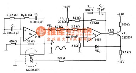
This diagram is wien bridge oscillator circuit controlled by photosensitive resistance. Usually it uses lamp and FET tube for the stability of wien bridge oscillator circuit amplitude. When you use lamp, the amplitude dynamic range can increase. But the response speed will become slow. When you use FET tube, the response speed will increase. But the amplitube dynamic range will become narrow. As the circuit shown in the figue 6-3, the amplitude stabilized element adopts optical coupler MCD521H composed of LED and photosensitive resistance to solve the problem. This is a kind of fast response, wide dynamic range and no mechanical vibration influence, quality oscillation circuit.
(View)
View full Circuit Diagram | Comments | Reading(1327)
IR_ILLUMINATOR_FOR_NIGHT_VISION_TV_CAMERAS_AND_SCOPES
Published:2009/6/19 4:10:00 Author:May
This Source uses LEDs and an astable oscillat to control the switch,duty-cycle,and effective IR illumination output. (View)
View full Circuit Diagram | Comments | Reading(1965)
Atomizer circuit
Published:2011/5/3 3:38:00 Author:May | Keyword: Atomizer
This article describes a device which can generate mirage around miniascape's rockwork and trees, like white clouds folating in the mountains, greatly improve the ornamental value.
一、 working principle
The circuit is show in the diagram.
This article describes a device which can generate mirage around miniascape's rockwork and trees which is seemingly as if white clouds floated in the mountains, and it greatly improves the ornamental value.
一、 working principle
The circuit is shown in the diagram.
It mainly consists of ultrasonic generator, the water level controller, power supply circuit etc. Ultrasonic generator mainly consists of triode VT1, VT1 and capacitor three-point LC oscillator composed of its outside component; B is ultrasonic transducer, its natural frequency fc=1.65MHz; capacitor C1, C2 can decide oscillation amplitude, its natural frequency is a little less than fc. L1 and C2 are positive feedback elements, and their natural is a little higher than fc; VD5 is protecting diode of VT1. B is under water when pulverization. Water level controller consists of VT2, VT3, the effect is:
(1) Offer base bias current for oscillation circuit;
(2)When the water level in the miniascape is lower than set value, it can make oscillator failure of oscillation and act the function of protection. (View)
View full Circuit Diagram | Comments | Reading(3117)
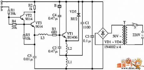
CAPACITOR_DISCHARGE_IGNITION_SYSTEM
Published:2009/6/19 2:31:00 Author:May
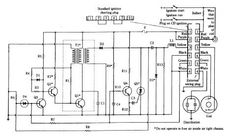
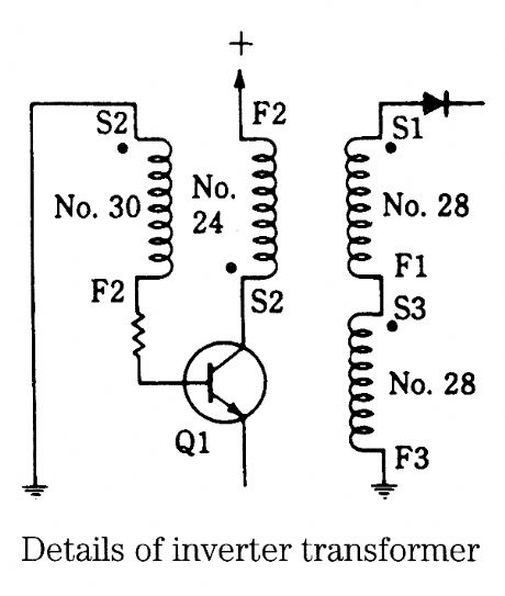
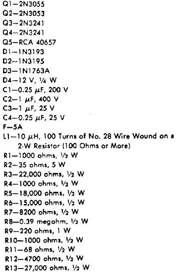
This ignition system charges a capacitor (C2) to 350 V and discharges it through the ignition coil. (View)
View full Circuit Diagram | Comments | Reading(1890)
STEREO_TV_DECODER
Published:2009/6/18 23:51:00 Author:May

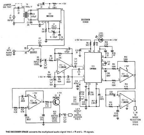
A block diagram of the stereo-TV decoder is shown in A. It shows the overall relationships be-tween the separate sections of the circuit; B through E show the details of each subsection. The de-coder section centers around IC1, a standard 4.5-MHz audio demodulator. The output of IC1 is routed to 51, which allows you to choose between the internally demodulated signal and an exter-nally demodulated one. Buffer amplifier IC2-a then provides a low-impedance source to drive IC3, an LM1800 stereo demodulator.When IC3 is locked on a stereo signal, the outputs presented at pins 4 and 5 are discrete left- and right-channel signals, respectively. In order to provide noise reduction to the L-R signal, you must recombine the discrete outputs into sum and difference signals. Op amp IC4-a is used to regenerate the L-R signal. It is wired as a difference amplifier, wherein the inputs are summed together (+L -,R). Capacitor C18 bridges the left- and right-channel outputs of the demodulator. Although it decreases high-frequency separation slightly, it also reduces high-frequency distortion.The L + R signal is taken from the LM1800 at pin 2, where it appears at the output of an internal buffer amplifier. The rawL -R signal is applied to IC4-b, a 12-kHz lowpass filter. The L + R signal is also fed through a 12-kHz low pass filter in order to keep the phase shift undergone by both signals equal.Next, the L - R signal is fed to Q2. It allows you to add a level control to the L - R signal path; it provides a low source impedance for driving the following circuits, and it inverts the signal 180°. In-version is necessary to compensate for the 180°inversion in the compander.Next comes the expander stage. At the collector of Q2 is a 75-μs de-emphasis network (R27 and C29) that functions just like the network that is associated with Q1. Note that Q2 feeds both Q3 and IC5-a, a -12-dB per octave high-pass filter. The output of that filter drives the rectifier input of IC6, an NE570. The 75-Hz high-pass filter at the rectifier input helps to prevent hum, 60-Hz sych buzz, and other low-frequency noise in the L - R signal from causing pumping or breathing.The NE570 contains an on-board op amp; its irtverting input is available directly at pin 5 and via a 20-kO series resistor at pin 6. The 18-kQ resistor (R30) combines with the internal resistor and C32 (0.01 μF) to form a first-order filter with a 390-μs time constant. Because the internal op amp oper-ates in the inverting mode, the -(L - R) signal is restored to the proper (L - R) form.The output of the expander drives another 75-Hz high-pass filter, but this one is a third-order type that provides -18 dB per octave rolloff. It is used to keep low-frequency noise from showing up at the output of the decoder. At this point, the (L - R) signal has been restored, more or less, to the condition it was in before it was dBx companded at the transmitter. (View)
View full Circuit Diagram | Comments | Reading(291)
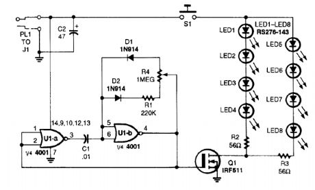
STEPPER_MOTOR_CIRCUIT_WITH_FET_DRIVERS
Published:2009/6/18 23:40:00 Author:May
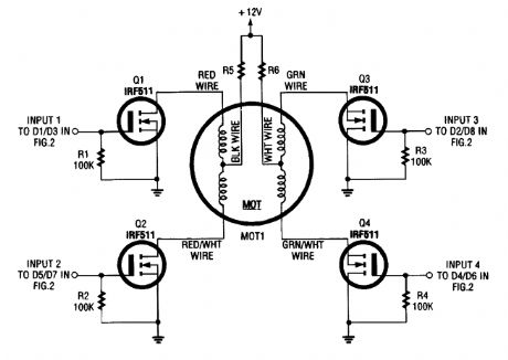
This motor-driver circuit replaces the eight bipolar transistors of the previous circuit with four IFR511 power hexFET's (Q1 through Q4). (View)
View full Circuit Diagram | Comments | Reading(1809)
ACTIVE_ANTENNA_FOR_UHF_SCANNERS
Published:2009/6/18 23:20:00 Author:May
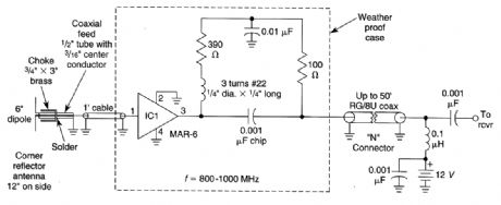
This active antenna IS a 1/2-wave dipole mounted In a 12"×12"×12"90°corner reflector,A builtin active preanlp IC1,fed dc through the RF coaxial line,provides 15 dB gain at 900 MHz to offset ca-ble losses,This provides supenor reception for scanners covering the 800- to 1000-MHz range. (View)
View full Circuit Diagram | Comments | Reading(719)
SPACE_AGE_SOUND_MACHINE
Published:2009/6/18 22:55:00 Author:May
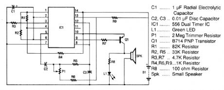
The space-age sound device uses a 556 dual-times IC to produce a phasor sound. That IC is ac-tually two 555 timer ICs in one 14-pin package, as shown in the schematic. Each timer inside the 556 is connected in an astable multivibrator mode.The first timer has its frequency set by R1, R2, and C1. Its output appears on pin 5 and it is cou-pled through C2 and R5 into the trigger input of the second timer. The second timer has an ad-justable frequency that is controlled by P1, R6, and C3.In the second timer, the first frequency mixes with the second frequency and produces the pha-sor-like sounds. The output of the second timer, which has the two signals mixed together, is brought from pin 9 through limiting resistor R7 to the input of Q1. The function of pnp gerrnanium power transistor Q1 is to amplify the signal to the level that is needed to drive the speaker. The green LED, L1, converts electrons directly into visible photons (light) in time with the pulses from the speaker. The purpose of resistor R8 is to limit the current through the LED to a safe level. (View)
View full Circuit Diagram | Comments | Reading(2474)
ATV_DOWNCONVERTER_FOR_420_TO_450_MHz
Published:2009/6/18 5:02:00 Author:May
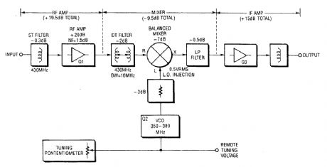
This ATV downconverter converts the 420- to 450-MHz ATV band, which is several channels be-tow the lower limit of the UHF band, to channel 3 or 4 for viewing on virtually any TV. The down-converter has a low-noise preamplifier stage and a double-balanced passive mixer for good performance and a wide dynamic range. That is necessary with today's crowded UHF bands. The converter draws about 27 milliamperes from a 13.2-volt dc source, so it can be used in portable and mobile applications. An extra IF stage gives an overall gain of about 25 dB. A block diagram of the clownconverter is also shown. A complete kit of parts, including PC board, is available from North Country Radio, P.O. Box 53, Wykagyl Station, New Rochelle, NY 10804-0053A. (View)
View full Circuit Diagram | Comments | Reading(2016)
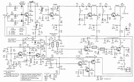
THREE_CHANNEL_420_TO_450_MHz_ATV_TRANSMITTER
Published:2009/6/18 4:59:00 Author:May
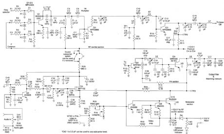
This transmitter is a 2-watt PEP output device for 420- to 450-MHz amateur TV operation. It has three crystal-controlled channels and will accept standard NTSC video input. It also has a 4.5-MHz sound subcarrier capability. Because this transmitter has AM modulation, audio can be transmitted in AM form on the RE carrier by applying audio to the video input. Bandwidth of audio can be restricted to 20 kHz by placing a 0.002-pF capacitor across R34. A complete kit of parts, including PC board is available from North Country Radio, P.O. Box 53, Wykagyl Station, New Rochelle, NY 10804-0053A. (View)
View full Circuit Diagram | Comments | Reading(2033)
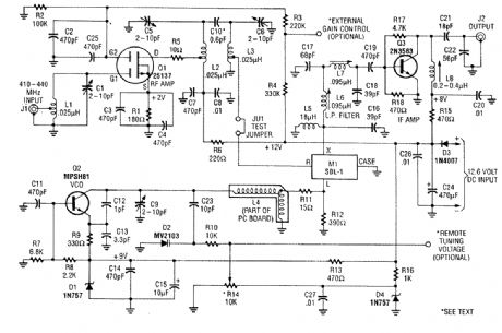
ATV_DOWNCONVERTER_FOR_902_TO_928_MHz
Published:2009/6/18 4:51:00 Author:May
This clownconverter converts ATV signals in the 902- to 928-MHz range to a 61.26- or 67.25-MHz IF output frequency (CH 3 or CH 4) to enable reception of these signals on a standard VHF TV receiver or monitor. It features a low-noise RF amp feeding a Schottky diode double-balanced mixer, a tunable LO and one IF preamp stage. The RF amplifier is a low-noise dual-gate GASFET that is followed by a sec-ond RE stage using an MMIC. Five tuned circuits are used in the RE amplifier. This feeds a packaged Schottlqr diode mixer assembly for better dynamic range and reduced susceptibility to intermodulation and strong signal areas. The on-board local oscillator (LO) is voltage tuned and if desired can be set up for remote tuning. Ail necessary circuitry for remote tuning is on board for coax dc and IF feed. This enables the clownconverter to be mast mounted to get around feedline losses generally associated with this frequency range. No separate dc feed is necessary because the coax (RG59/U recommended) carries dc power, tuning voltage, and IF signal. A dc block is used at the receiver for the purpose of separating dc voltage supply and the tuningvoltage. This allows a cable run of several hundred feet, if needed.By using this clownconverter and transmitter, a physically small915-MHz ATV station or even a video HT can be constructed because both units are each 2.50 x 4.00 inches x 1.00 high, and can be stacked together. A complete kit of parts, including PC board is available from North Country Radio, P.O. Box 53, Wykagyl Station, New Rochelle, NY 10804-0053A. (View)
View full Circuit Diagram | Comments | Reading(1482)
THREE_CHANNEL_902_TO_928_MHz_ATV_TRANSMITTER
Published:2009/6/18 4:42:00 Author:May
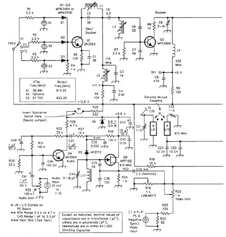
This transmitter is for ATV applications in the 902- to 928-MHz band. It has three crystal-con-trolled channels, and will accept standard NTSC video input. It also has a 4.5-MHz sound subcarrier.Because this is an lNI transmitter, audio can be transmitted as AM on the RF carrier. Simply use the video input Bandwidth。f audio can be restricted to dU kHz by placing a capacitor with a value of about o.002 pF across R34 The output is 1 5 to 2 watts PEP into a 50-Ω load,A complete kit of partsincluding PC board,is available from North Country Radio,P.O 0.Box 53,Wyktation,New Rochelle,NY 10804-0053A (View)
View full Circuit Diagram | Comments | Reading(1830)
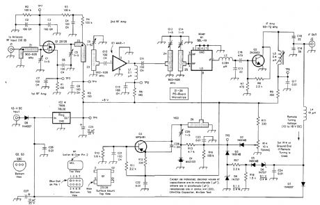
MAST_MOUNTED_ATV_PREAMP
Published:2009/6/18 4:29:00 Author:May
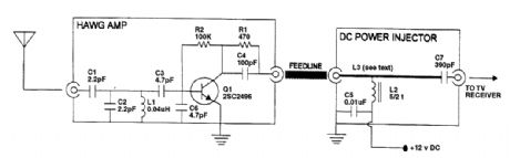
This simple ATV preamp covers the 427-to 439-MHz ATV frequencies and can be mast mounted and dc powered through the feedline. (View)
View full Circuit Diagram | Comments | Reading(1032)
MINI_ATV_TRANSMITTER
Published:2009/6/18 3:52:00 Author:May
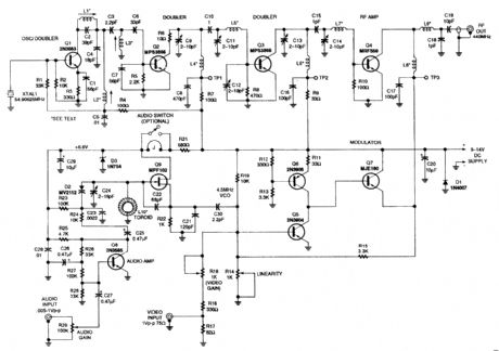
This low-power NTSC video and sound transmitter is useful for amateur radio, video handle-talkie, R/C and surveillance pur-poses. A crystal oscillator-multip lier RI' power amplifier. Video modulation is via a three-transistor series modulator. The sound subcarrier is generated with a VC0 circuit and is combined with the video information. The output is 0.4 to 1.2 W with supply volt-ages of 9 to 14 volts. A complete kit of parts, including PC board, is available from North Country Radio, P.O. Box 53, Wykagyl Sta-tion, New Rochelle, NY 10804-0053A. (View)
View full Circuit Diagram | Comments | Reading(2885)
| Pages:84/126 At 2081828384858687888990919293949596979899100Under 20 |
Circuit Categories
power supply circuit
Amplifier Circuit
Basic Circuit
LED and Light Circuit
Sensor Circuit
Signal Processing
Electrical Equipment Circuit
Control Circuit
Remote Control Circuit
A/D-D/A Converter Circuit
Audio Circuit
Measuring and Test Circuit
Communication Circuit
Computer-Related Circuit
555 Circuit
Automotive Circuit
Repairing Circuit