
LED and Light Circuit
Index 45
SEQUENTIAL_FLASHER
Published:2009/7/9 2:00:00 Author:May
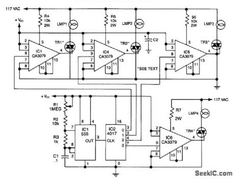
Using a 555 timer to drive a CMOS counter, this device uses RCA CA3079 zero-voltage switch to control triacs TRI through TR4. This circuit can be used to sequence lamp displays, etc.
Caution: The CA3079s are connected to the 117-V line, as is the clock and counter circuit and their power supplies. Use caution, good insulation, and safe construction practices. (View)
View full Circuit Diagram | Comments | Reading(0)
MARK_SENSOR_FOR_CARDS
Published:2009/7/20 10:23:00 Author:Jessie
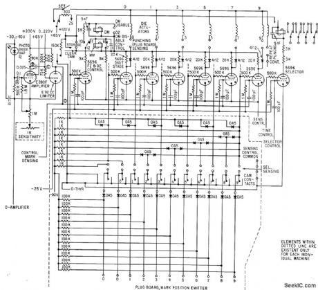
Automatically transcribes up to 40 pencil marks on specially printed 90-column cards into machine code and block-punches information into cards in any desired format at 150 cards per minute -F. A. Frankl, Transcribing Field Markings by Optical Scanning, Electronics, 34:31, p 49-51. (View)
View full Circuit Diagram | Comments | Reading(1745)
LAMP_PREHEATER
Published:2009/7/20 10:11:00 Author:Jessie
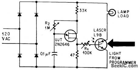
Unijunction transistor triggers LASCR (light-activated scr) late in each half-cycle, with R2 determining lamp current so filament is heated but not visible. This preheating minimizes thermal stresses during programmed operation of lamps by control beam hitting LASCR, as for theaters or fountains.-E. K. Howell, Light-Activated Switch Expands Uses of Silicon-Controlled Rectifiers, Electronics, 37:15, p 53-61. (View)
View full Circuit Diagram | Comments | Reading(1482)
NOISE_SUPPRESSOR
Published:2009/7/20 10:10:00 Author:Jessie
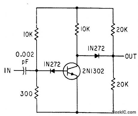
Removes noise from output of photodiode used in reflected-light shaft-position encoder. -F. W. Kear, How to Select Shaft-Position Encoders, Electronics, 35:35, p 48-51. (View)
View full Circuit Diagram | Comments | Reading(2212)
A_C_MODULATOR_FOR_PHOTOMULTIPLIER
Published:2009/7/20 8:03:00 Author:Jessie
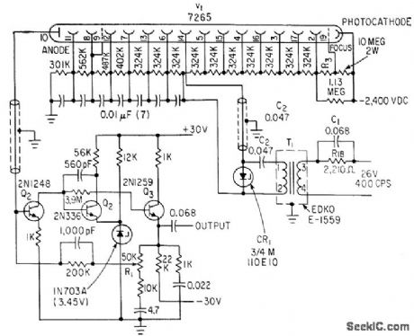
Output of star-tracking photomultiplier is converted to a-c by applying 400-cps modulating voltage to dynode 14, to make gain vary between nominal value and 1% of this in square wave fashion. Amplifier passband is then 130 to 800 cps.-E. R. Schlesinger, Aiming a 3-Ton Telescope Hanging from Balloon, Electronics, 36:6, p 47-51. (View)
View full Circuit Diagram | Comments | Reading(971)
AUTOMATIC_CALIPER
Published:2009/7/20 7:58:00 Author:Jessie
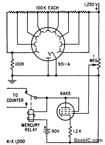
Photomultiplier and counter circuit on machine lathe feed recorder to give dimensions of printed circuits and photographic plates in increments of 0.0001 inch.-S. Isaacson, Electronic Caliper Checks Printed Circuits, Electronics, 32:1, p 44-45. (View)
View full Circuit Diagram | Comments | Reading(741)
_EIGHT_OHANNEL_VOLTAGE_DISPLAY
Published:2009/7/9 1:57:00 Author:May
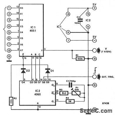
This circuit turns a common oscilloscope into a versatile eight-channel display for direct voltages. The trend of each of the eight input levels is readily observed, albeit that the attainable resolution is not very high.
The circuit diagram shows the use of an eight-channel analog multiplexer IC1, which is the electronic version of an eight-way rotary switch with contacts X0 through X7 and pole Y. The relevant channel is selected by applying a binary code to the A-B-C inputs. For example, binary code 011 (A-B-C) enables channel 7 ( X6 Y ). The A-B-C inputs of IC1 are driven from three successive outputs of binary counter IC2, which is set to oscillate at about 50 kHz with the aid of P1. Since the counter is not reset, the binary state of outputs Q5, Q6, and Q7 steps from 0 to 7 in a cyclic manner. Each of the direct voltages at input terminals 1 to 8 is therefore briefly connected to the Y input of the oscilloscope. All eight input levels can be seen simultaneously by setting the timebase of the scope, in accordance with the time it takes the counter to output states 0 through 7, on outputs Q5, Q6, and Q7.
The timebase on the scope should be set to 0.5 ms/div, and triggering should occur on the positive edge of the external signal. Set the vertical sensitivity to 1 V/div. The input range of this circuit is from -4 V to +4 V; connected channels are terminated in about 100 KΩ. (View)
View full Circuit Diagram | Comments | Reading(1238)
CORONAMETER
Published:2009/7/20 7:48:00 Author:Jessie
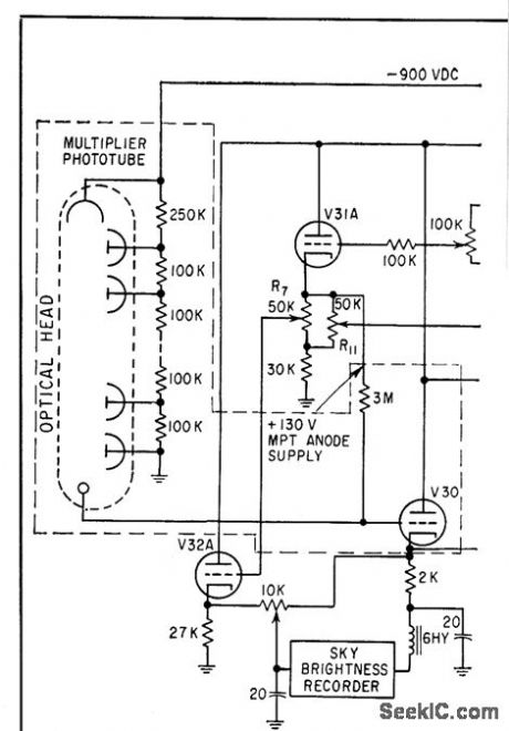
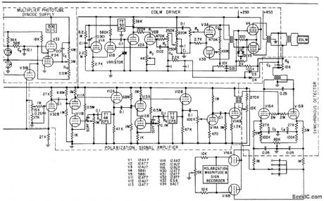
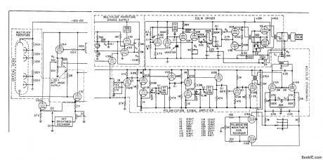
Uses polarized-light technique and closely controlled narrowband circuit to detect, observe, and measure otherwise invisible solar phenomenon. Circuit shows multiplier tube in optical head, with dynode supply, electro-optical light modulator (EOLM) driver amplifiers, polarization signal amplifier, and synchronous detector.-R. H. Lee and J. G. Fullerton, K-Coronameter Observes the Sun's Electron Corona, Electronics, 34:47, p 58-62. (View)
View full Circuit Diagram | Comments | Reading(1375)
INDICATOR_LAMP_DRIVER
Published:2009/7/8 22:43:00 Author:May
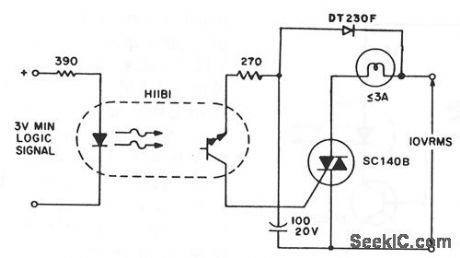
A simple solid-state relay circuit drives the 10-Vac telephone indicator lamps from logic circuitry, while maintaining complete isolation between the 10-V line and the logic circuit. (View)
View full Circuit Diagram | Comments | Reading(787)
HEAT_ENERGY_INTEGRATOR
Published:2009/7/8 5:19:00 Author:May
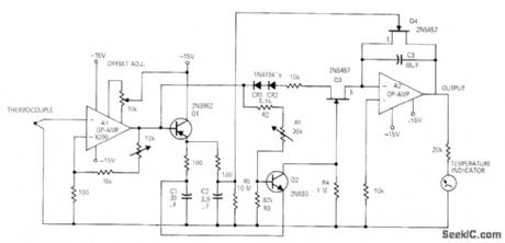

Pulses of heat energy applied to solder preforms by tips of pulsed soldering machine are metered by integrate/hold-to-indicate circuit using thermocouple as input sensor. Temperature derived from area under time/temperature curve is indicated momentarily on output meter, as guide for operator when size of solder preform is changed.Article describes operation of circuit in detail and gives timing diagram.—C Brogado,Heat-Energy Pulse Measured and Displayed,EDN Magazine,Sept,15,1970,p 61-62. (View)
View full Circuit Diagram | Comments | Reading(940)
3_digit_ISUP2_SUPL_DPM_with_LED_CPU_interface
Published:2009/7/20 22:13:00 Author:Jessie
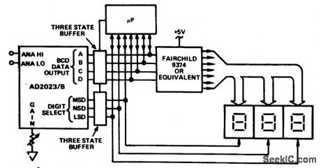
3-digit I2L DPM with LED/CPU interface(courtesy Analog Devices, Inc.). (View)
View full Circuit Diagram | Comments | Reading(727)
FEEDBACK_REDUCES_DRIFT
Published:2009/7/20 21:54:00 Author:Jessie
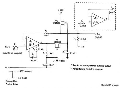
FET Q2 serves as buffer for hold capacitor C1, minimizing droop error. Switching transistorQ1 is placed in feed-back loop. A1 serves as input signal buffer and as driver for Q1 and C1. When sample line is raised to +15 V by control pulse, D1 is reverse-biased and a, is turned on C1 now charges until output terminal reaches equilibrium with input (so A1 is tracking input). When sample pulse goes low, feedback loop of A1 is opened; output of A1 stays at voltage last sampled since C1 retains its charge and Q2 buffers this voltage while presenting it to output. Optional voltage follower can be used if more output current is needed to feed low-impedance load.-W. G. Jung, IC 0p-Amp Cookbook, Howard W. Sams, Indianapolis, IN, 1974, p 198-200. (View)
View full Circuit Diagram | Comments | Reading(693)
LC_CHECKER
Published:2009/7/7 23:03:00 Author:May
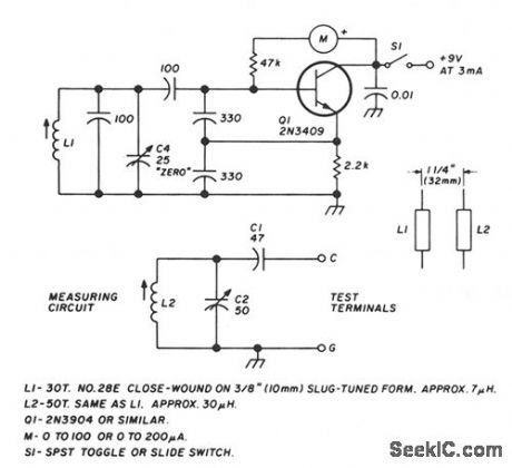
The circuit is based on the grid-dip or absorption effect, which occurs when a parallel resonant circuit is coupled to an oscillator of the same frequency. Q1 operates in a conventional Colpitts oscillator circuit at a ftxed frequency of approximately 4 MHz. A meter connected in series with the transistor's base-bias resistor serves as the dip or absorption indicator.The variable measuring circuit consists of C1, C2, and L2 and is connected to panel terminals as shown. L2 is loosely coupled to L1 in the oscillator circuit. This measuring circuit is tuned to the oscillator frequency with variable capacitor C2 set at full capacitance. When power is applied to the oscillator, the meter shows a dip caused by power absorption from the measuring circuit.Connecting an unknown capacitor across the test terminals lowers the resonant frequency of the measuring circuit. To restore resonance, tune capacitor C2 lower in capacitance. The meter will dip again when you reach this point. Determine the capacitance across the text terminals by calibrating the dial settings of C2.Capacitor C4, a small variable trimmer in the oscillator circuit, compensates for drift or other variations and is normally set at half capacitance. The capacitor is a panel control, labeled zero, and it is used to set the oscillator exactly at the dip point when C2 is set at maximum capacitance. This corresponds to zero on the calibration scale.
(View)
View full Circuit Diagram | Comments | Reading(3733)
LED_PEAKMETER
Published:2009/7/7 22:59:00 Author:May
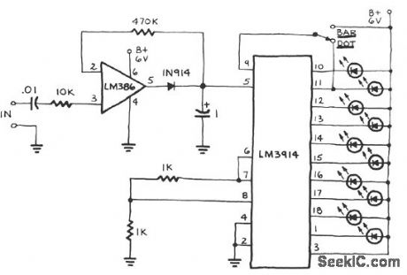
The circuit includes a peak detector that immediately drives the readout to any new higher signal level and slowly lowers it after the signal drops to zero. The readout is a moving dot or expanding bar display.The circuit can be expanded for a longer bar readout. Tapping five or more LED peakmeters into a frequency equalizer or series of audio filters should give a unique result. The bottom LED remains on with no signal at the input, thus providing a pilot light for the unit. (View)
View full Circuit Diagram | Comments | Reading(1548)
LED_DIE
Published:2009/7/7 22:54:00 Author:May
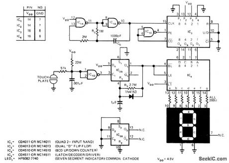
When positive bias on input of IC1D number displayed. Number can be between 1 NAND gate is puiied to ground by skin resistance of finger, D flip-flop IC2A connected as mono is triggered. Pin 1 goes high for about 2 s, making IC4. latch outputs of counter IC3 andunblank LED display. Randomtime that fingeris on touch plate determines randomness of number displayed. Number can be between 1 and9, between 1 and 6 for die,between 1 and2 to representheads or tailsChange BCDof jam inputs of IC3 to highest random number desired .Values shown are for 4.5-V supply and dispiay current of 10 mA PER SEGMENT. LEDisblanked until plateis touched Standby current drain of 10 μA on three AA alkaline cellsis so low that ON/OFF switch is unnecessary.-C,Cullings,Electronic Die Uses Touchplate and 7Segment LED Disρlay,EDN Magazine,May 20,1975、p70 and 72. (View)
View full Circuit Diagram | Comments | Reading(1488)
SCOER_DISPLAY
Published:2009/7/7 21:52:00 Author:May
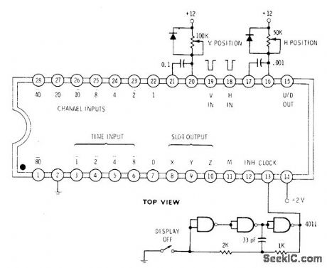
National 5841 IC is used for display of video game scores on TV receiver, as well as for time and channel number displays.Properly conditioned H and V pulses must be applied to pins 18 and 19 to interface TV. Output video on pin 15 must be buffered and summed into existing video inside TV set. Display position is controlled by H and V pots. Horizontal display size depends on clock frequency.Grounding M input gives only channel number.Positive voltage at M gives both channel and time. Grounding D input provides 5-slot time display, while positive D input gives 8-slot time display. Channel inputs are applied continuously in negative-logic form, with time inputs multiplexed externally.-D. Lancaster, CMOS Cookbook, Howard W. Sams, Indianapolis, IN, 1977, p 158. (View)
View full Circuit Diagram | Comments | Reading(1079)
WARNING_LIGHTAND_MARKER_LIGHT
Published:2009/7/7 21:26:00 Author:May
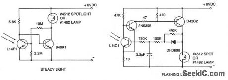
A flashing light of high brightness and short duty cycle is often desired to provide maximum visibility and battery life. This necessitates using an output transistor, which can supply the cold filament surge current of the lamp while maintaining a low saturation voltage. The oscillation period and flash duration are determined in the feedback loop, while the use of a phototransistor sensor minimizes sensitivity varia-tions. (View)
View full Circuit Diagram | Comments | Reading(909)
800_W_SOFT_START_LIGHT_DIMMER
Published:2009/7/7 9:50:00 Author:May
The zener provides a constant voltage of 20 V to unijunction transistor Q1, except at the end of each half-cycle of the input when the line voltage drops to zero. Initially, the voltage across capacitor C1 is zero and capacitor C2 cannot charge to trigger Q1. C1 will begin to charge, but because the voltage is low, C2 will be charged to a voltage adequate to trigger C1 only near the end of the half cycle. Although the lamp resistance is low at this time, the voltage applied to the lamp is low and the inrush current is small. Then the voltage on C1 rises, allowing C2 to trigger Q1 earlier in the cycle. At the same time, the lamp is being heated by the slowly increasing applied voltage. By the time the peak voltage applied to the lamp has reached its maximum value, the bulb has been heated sufficiently to keep the peak inrush current at a reasonable value. Resistor R4 controls the charging rate of C2 and provides the means to dim the lamp. Diode D6 and resistor R7 improve operation at low-conduction angles. (View)
View full Circuit Diagram | Comments | Reading(0)
ON_THE_AIR_INDICATOR
Published:2009/7/7 8:08:00 Author:May
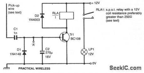
The circuit is a simple rf-actuated switch which will respond to any strong fteld in the region of the pickup wire. The length of the wire will depend on how much coupling is needed, but a 250-mm length wrapped around the outside of the coaxial cable feeding the antenna should sufflce for most power levels. If only one band is used, the wire can be made a resonant length-495 mm for 144 MHz band operation for example. When rf energy is picked up by the device, diode D1 will conduct on the negative half-cycles, but will be cut off on the positive half-cycles. The result will be a net positive voltage at the base of transistor Tr1, forward biasing it into conduction. On ssb and cw transmissions, where the transmission is not continuous, that bias would be constantly varying and the relay RLA would chatter. However, capacitor C2 holds the bias voltage steady until a long gap in transmissions occurs. (View)
View full Circuit Diagram | Comments | Reading(1077)
VISUAL_LEVEL_INDICATOR
Published:2009/7/7 8:05:00 Author:May
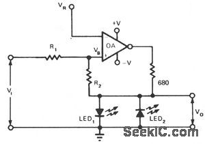


This indicator is basically a switch with hysteresis characteristics. If the input voltage momentarily (or permanently) exceeds the most positive refer-ence level, LED1 is switched on. If, on the other hand, the voltage falls below the negative, or least positive, reference level, LED1 will be switched off and LED2 switched on. The output voltage, VO is clamped either to the diode voltage VD1 , orVD2 depending on which LED is conducting. ForVO to be positive, VB has to be positive with respect to the reference voltage VR; for VO to be negative, VB has to be negative with respect to VR. (View)
View full Circuit Diagram | Comments | Reading(799)
| Pages:45/72 At 204142434445464748495051525354555657585960Under 20 |
Circuit Categories
power supply circuit
Amplifier Circuit
Basic Circuit
LED and Light Circuit
Sensor Circuit
Signal Processing
Electrical Equipment Circuit
Control Circuit
Remote Control Circuit
A/D-D/A Converter Circuit
Audio Circuit
Measuring and Test Circuit
Communication Circuit
Computer-Related Circuit
555 Circuit
Automotive Circuit
Repairing Circuit