
LED and Light Circuit
Index 58
Five flash lamp string circuit (1)(M1500P)
Published:2011/7/5 22:08:00 Author:zj | Keyword: Five flash, lamp string circuit
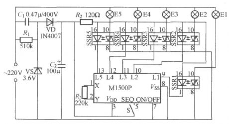
As shown in the figure itis five flash lamp string controller made by M1500P five flash integrated circuit produced by ShenzhenSkywave semiconductor limited Company. M1500P uses the CMOS process, it uses the power supply voltage standard values for 3V, L1 ~ L5 five output end can be directly driven LED blinking, flashing mode there are random and continuous two options are available. SSR1 to SSR5 uses TAC081 IC type solid state relay. Its maximum load currentis 1A. (View)
View full Circuit Diagram | Comments | Reading(667)
Practical delay lamp circuit (3)
Published:2011/7/6 20:58:00 Author:zj | Keyword: Practical, delay lamp
As the diagram shows, it is a delay light controllor with good performance. The connection betweenthe controller and the lamp is two wire type. The installation and the using is very convenient. And there is no special requirement for components. (View)
View full Circuit Diagram | Comments | Reading(706)
Practical delay lamp circuit (2)
Published:2011/7/6 21:02:00 Author:zj | Keyword: Practical, delay lamp circuit
View full Circuit Diagram | Comments | Reading(619)
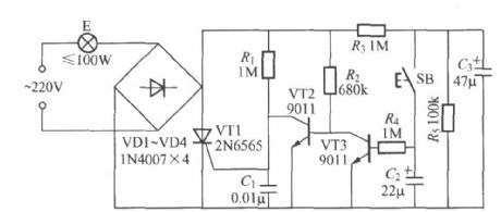
Practical delay lamp circuit (1)
Published:2011/7/6 21:13:00 Author:zj | Keyword: Practical, delay lamp circuit
As the diagram shows it is a practical delay light controllor suitable for staircase aisle or toilet. When you press the switch SB down, it will light up for a few minutes. Then after that it will go out. (View)
View full Circuit Diagram | Comments | Reading(658)
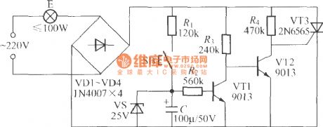
Delay lamp circuit using relay (3)
Published:2011/7/6 22:50:00 Author:zj | Keyword: Delay lamp circuit, using relay
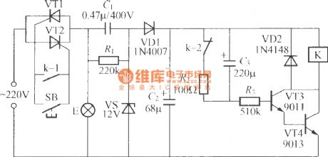
As shown in the figue, VT1, VT2 can adopt two 1A / 400V type unidirectional thyristors with the same properties. K can use JRX-13F, DC12V type miniature electromagnetic relay, which has two sets of switch contacts, and can meet the requirements. (View)
View full Circuit Diagram | Comments | Reading(640)
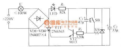
Delay lamp circuit using relay (2)
Published:2011/7/7 2:02:00 Author:zj | Keyword: Delay lamp circuit, using relay
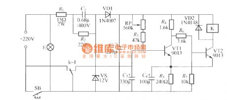
As the figue shows, it is a delay lamp circuit using relay with good perfomance. Press down SB to makelamp E light. At the same time,the 220V AC passes capacitance step-down half-wave rectifying and voltage-stabilizing circuit composed of VS, VD1,C1,C2.The C2 ends outputvoltage is 12V. Three transistor VT1 base is relay contact k-1 grounding and stop, so VT2 conductive, electric relay K. Contact k-1 backward often start, the key SB short circuit self-locking, so the release SB, light E can still be energized to emit light. The positive power supply by RP, R3 to C3 the VT1 capacitor charging base potential gradually raised, when raised to a certain degree, the VT1 conduction, VT2 VT1, VT2 cutoff, which consists of the Schmidt circuit turned back to the original state, the relay K release, contact k-1 reset lamp E power supply circuit is cut off and the lights went out. (View)
View full Circuit Diagram | Comments | Reading(1131)
CS7232 touch-free dimming light circuit 1
Published:2011/5/11 4:05:00 Author:May | Keyword: touch-free, dimming light
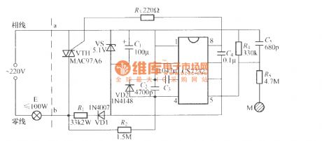
The diagram shows touch-free dimming light made of CS7232 dimming application specific integrated circuit. Touch M can adjust the light of lamp E with none stage. (View)
View full Circuit Diagram | Comments | Reading(995)
AUDIO_LIGHT
Published:2009/6/18 22:30:00 Author:May
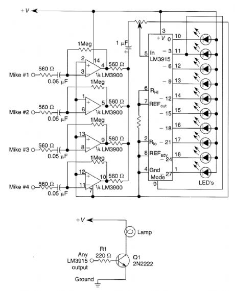
This circuit will produce an output when the sound exceeds a preset level. The LM3915 is a log-output bar graph driver. Use the transistor driver shown for higher current loads. To drive heavy-current loads with an LM3915 output, you must add a transistor, as shown in B. (View)
View full Circuit Diagram | Comments | Reading(2462)
SIMPLE_NEON_LIGHT_DRIVER
Published:2009/6/18 4:44:00 Author:May
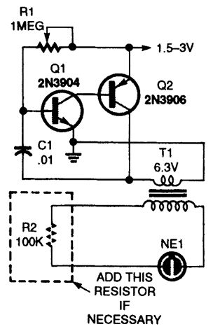
NE1, a neon lamp, is lit by this simple inverter circuit. T1 is a 20:1 tum ratio transformer (transistor radio output, etc.). (View)
View full Circuit Diagram | Comments | Reading(1725)
LED_BARGRAPH_DRIVER_CIRCUIT
Published:2009/6/18 4:28:00 Author:May
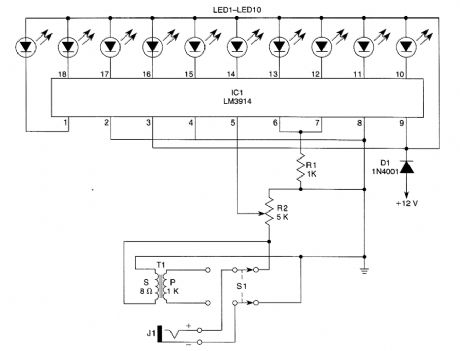
This circuit is used as an audio indicator. S1 selects direct input or a 1-kΩ(high impedance) audio input. R2 is a sensitivity control. (View)
View full Circuit Diagram | Comments | Reading(1024)
LCD_CONTRAST_TEMPERATURE_COMPENSATOR
Published:2009/6/18 4:26:00 Author:May
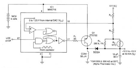
Negative temperature-coefficient resistor R5 modifies feedback in this switching regulator, which results in a negative output voltage that varies with temperature. With properly chosen resistor values, the circuit produces a temperature compensated bias voltage that ensures constant con-trast in an LCD. (View)
View full Circuit Diagram | Comments | Reading(1079)
SIMPLE_COLOR_ORGAN
Published:2009/6/18 4:21:00 Author:May
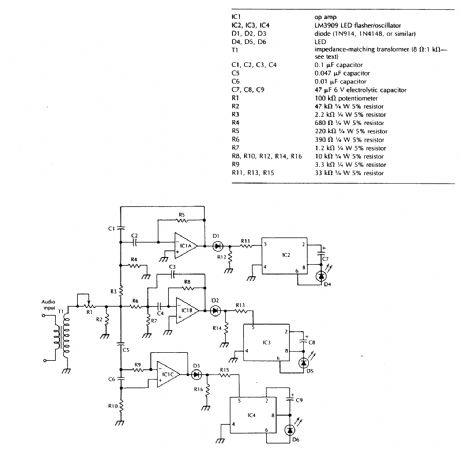
Three active filters that divide the audio spectrum into three bands drive rectifiers and then drive IC2, 3, and 4, flashing the LEDs at 6 Hz. D4, D5, and D6 should be three different colors for best effect. (View)
View full Circuit Diagram | Comments | Reading(1814)
STEREO_LEVEL_DISPLAY
Published:2009/6/18 4:16:00 Author:May
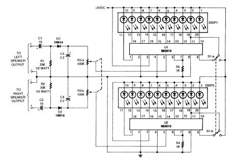
Two bar graph drivers and LEDs are used in this volume (level) indicator. R3a and R3b set the sensitivity of the circuit. The LEDs can be either bar graph units or individual LEDs can be used. (View)
View full Circuit Diagram | Comments | Reading(2536)
COLOR_SHIFTING_LED_DISPLAY
Published:2009/6/18 4:14:00 Author:May
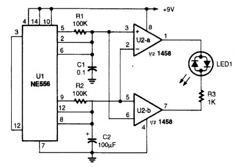
This circuit is used to make a tricolor LED gradually change color from yellow to red to yellow to green, and then back to yellow, where the cyclerepeats. It is very simple to make, and the theory of operation is also simple. Both of the timers in the556 dual oscillator/timer are configured for astable operation with a 50% duty cycle. 0ne timer is set uEDt to oscillate much faster than the other. The timing capacitor voltage of each is sent to two comparators, which apply a voltage across the tri-color LED whose polarity depends on which capacitor voltageis higher. The rapidly changing capacitor's voltage causes the red and green elements of the LED tobe altemately lit, thus giving the illusion of yeilow light. As the slowly rising and faLing voltage from the slower trimming capacitor changes in average value, it shifts the duty cycle to favor one color or the other. That gives the transition between colors a smooth appearance. (View)
View full Circuit Diagram | Comments | Reading(1913)
LOGIC_STATE_CHANGE_INDICATOR
Published:2009/6/18 3:07:00 Author:May

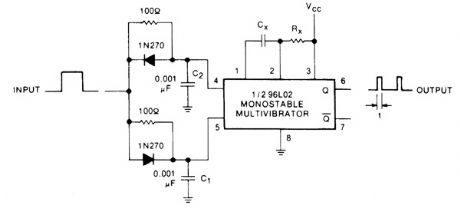


A circuit consisting of a one-shot multivibrator IC, a pair of diodes, and some resistors and capacitors delivers an output pulse when the logic state at its input terminal changes-either from high to low or from low to high. Thus, this circuit can serve as a state-change indicator or as a frequency doubler for a square-wave input.Any monostable can be used; the arrangement in the figure achieves low power dissipation(80 milliwatts)by using half of a Fairchild 96L02 transistor-transistor-logic dual multivibrator. The 96L02 is triggered when pins 3 and 5 are high and pin 4 changes state from low to high. It also triggers if pin 3 is high, pin 4 is low.The circuit shown here allows these conditions to be satisfied with a single input terminal, plus the fixed bias on pin 3; the arrangement of resistors, capacitors, and diodes automatically biases pin 5 high when transmitting a rising transition to pin 4 and biases pin 4 low when applying a falling tran-sition to pin 5.For example, if the input terminal has been low and then goes high, C1 charges through a for-ward-biased diode that shunts its 100-Ω resistor; therefore pin 5 goes high immediately. C2 charges through 100 Q; however, because its diode is back-biased, the rising level is not applied to pin 4 un-tilSis already high. Therefore, the conditions for triggering an output pulse are satisfied.The output pulse duration, f, is set by the value of time constant RXCX. (View)
View full Circuit Diagram | Comments | Reading(856)
PROGRAMMABLE_CW_IDENTIFIER_
Published:2009/6/18 2:37:00 Author:May
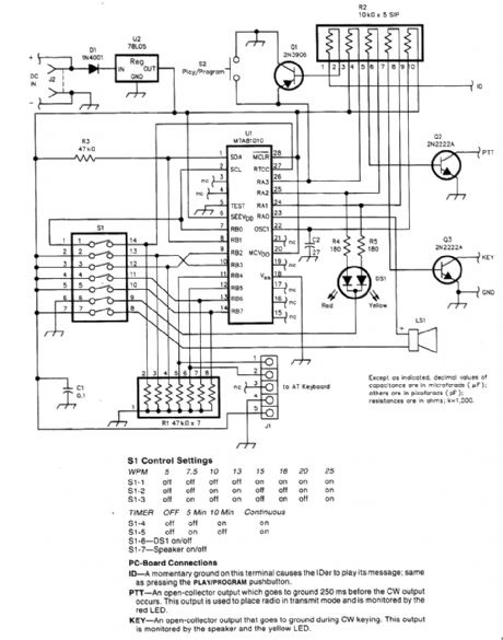
The identifier uses an MTA81010 microchip,containing a 1024-bit serial EEPROM and a rmcro-controlier It runs from a 9-V battery.A standard AT-type keyboard is used to progran the desiredmessage Speed varles from 5 to 25 wpm. (View)
View full Circuit Diagram | Comments | Reading(744)
FLASHING_BRAKE_LIGHT_FOR_MOTORCYCLES
Published:2009/6/17 23:31:00 Author:May
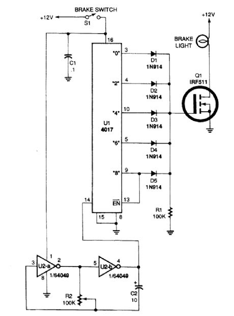
When brake-light switch 51 is closed, power is applied to UI and U2. Two inverters of U2, a 4049 hex inverting buffer, are connected in a low-frequency oscillator circuit that feeds clock pulses into UI, a 4017 decade counter/divider. Outputs 0, 2, 4, 6, and 8 of U1 are coupled to the gate of Ql through a 1N914 diode. As the 4017 counts down, it turns the brake light on and offfour times and then leaves it on until the brake switch is released. The on/off rate can be set by potentiometer R2; for best results, the on/off rate should be set so that it is rapid. (View)
View full Circuit Diagram | Comments | Reading(1331)
OVERLOAD_INDICATOR
Published:2009/6/17 20:42:00 Author:May
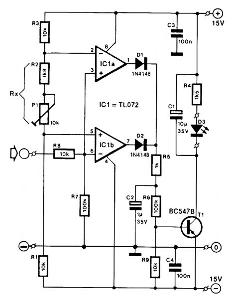
Two op amps are used as comparators to indi-cate excessive magnitude of an AP signal, either positive or negative, even if the signal is asymmet-rical. P1 sets the reference voltage for both op amps. This circuit is useful for audio-amplifier and op-amp circuits using split power supplies. (View)
View full Circuit Diagram | Comments | Reading(1377)
BATTERY_OPERATED_BLACK_LIGHT
Published:2009/6/17 2:48:00 Author:May
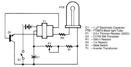
The battery-operated blagk light uses a “U”-shaped, unfiltered, black-light tube, which requires approximately 250 Vac to operate. To create the 250-Vac 6-V battery, the circuit uses a one-transis-tor blocking oscillator that drives a ferrite inverter transformer. A blocking oscillator tums itself off after one or more cycles. In this circuit, it consists of C1, P1, Q1, R1, and T1. The oscillations are sus-tained because the base of Q1 is connected to one of the windings on T1.Transformer T1 is a step-up transformer that consists of a ferrite core, which has a few tums on the primary and many turns on the secondary. The oscillating (ac) output of Q1 is fed to T1, which, because of its large tums ratio, converts the low-voltage signal into a high-voltage altemating cur-rent, which is coupled through resistor R2 to the black-light tube. Resistor R1 and trimmer resistor P1 limit the current flowing through the circuit. As the control on P1 is rotated, more current flows in the circuit, producing a brighter light output. (View)
View full Circuit Diagram | Comments | Reading(2269)
PHOTOTRANSISTOR_CIRCUITS
Published:2009/6/17 2:43:00 Author:May
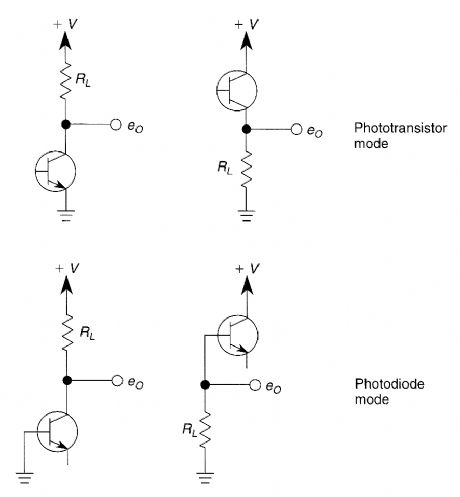
Here are four ways to connect a phototran-sistor for general use in phototransistor circuits. (View)
View full Circuit Diagram | Comments | Reading(1656)
| Pages:58/72 At 204142434445464748495051525354555657585960Under 20 |
Circuit Categories
power supply circuit
Amplifier Circuit
Basic Circuit
LED and Light Circuit
Sensor Circuit
Signal Processing
Electrical Equipment Circuit
Control Circuit
Remote Control Circuit
A/D-D/A Converter Circuit
Audio Circuit
Measuring and Test Circuit
Communication Circuit
Computer-Related Circuit
555 Circuit
Automotive Circuit
Repairing Circuit