
LED and Light Circuit
Index 46
STEREO_INDICATOR
Published:2009/7/7 8:00:00 Author:May

On most FM tuners, the stereo indicator lights upon detection of the 19-kHz pilot tone. However, this doesn't mean that the program is actually stereophonic, since the pilot tone is often transmitted with mono programs also. A similar situation exists on stereo amplifiers, where the stereo LED is simply con-trolled from the mono/stereo switch.The LED-based stereo indicator described here lights only when a true stereo signal is fed to the inputs. Differential amplifier A1 raises the difference between the L and R input signals. When these are equal, the output of A1 remains at the same potential as the output of A2, which forms a virtual ground rail at half the supply voltage. When A1 detects a difference between the L and R input signals, it supplies a positive or negative voltage with respect to the virtual ground rail, and so causes C3 to be charged via D1 or C4 via D2. Comparator A3/A4 switches on the LED driver via OR circuit D3/D4. The input signal level should not be less than 100 mV to compensate for the drop across Dl or D2. The sensitivity of the stereo indicator is adjustable with P1. (View)
View full Circuit Diagram | Comments | Reading(1543)
MULTIPLEXING_OF_DISPLAYS
Published:2009/7/7 5:06:00 Author:May
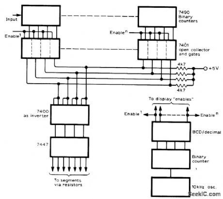
Three or more displays can be multiplexed simply by gating 7490 counter output via 7401, then using OR connection for outputs. 7401s are switched on in rotation by positive enable signal which also switches displays on in turn. If using common-cathode displays, segment and display enable signals must be inverted. With individual display units, segments must be paralleled.-G. A. Bobker, Simplified Multiplexing, Wireless World, Feb. 1978, p 59. (View)
View full Circuit Diagram | Comments | Reading(1016)
BCD_FROM_7_SEGMENT_DISPLAY
Published:2009/7/7 4:56:00 Author:May
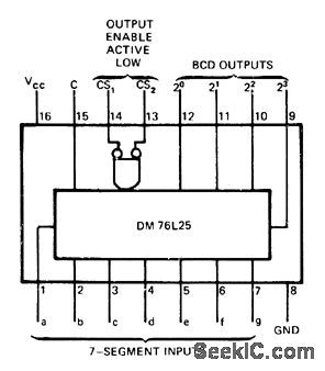
Single National DM76L25 read-only memory provides conversion from 7-segment outputs of MOS chip driving display to BCD inputs for data processing. Typical power dissipation is 75 mW. Access time is 70 ns when using 5-V supply. Article gives truth table for all standard and special characters of 7-segment display.-U. Priel, 7-Segment-to-BCD Converter: The Last Word?, EDN Magazine, Aug. 20, 1974, p 94-95. (View)
View full Circuit Diagram | Comments | Reading(2145)
MOTOR_STEP_ANGLE_DISPLAY
Published:2009/7/7 4:12:00 Author:May

DigitaI display circuit tracks stepper-motor shaft movements. Up/down decade counters read out four BCD digits as travel angle (000.0 to 360.0) in degrees and number of completed revolutions (0 to 9). Stepper under study is driven by state generator that produces high-current square-wave pulses under control of clock used for display, which can be external square-wave generator or clock output of microprocessor such as KIM-1:. Power source for digital display is 5 V at 1.2 A. Applications include monitoring movements of incremental plotters, precision film camera drives, numerical control machines, and precision start-stop motions of fuel control rods in nuclear reactor.-H. Lo, Digital Display of Stepper Motor Rotation, Computer Design, April1978, p 147-148 and 150-151.
(View)
View full Circuit Diagram | Comments | Reading(2242)
EIGHT_DIGIT_MICROPROCESSOR_DISPLAY
Published:2009/7/7 3:29:00 Author:May
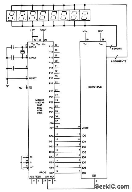
Display interface uses the ICM7218A/B with an 8048 family microcontroller. The 8-bit data bus (DB0/ DB7-ID0/ID7) transfers control and data information to the 7218 display interface on successive WRITE pulses. The mode input pins on the microcontroller. When mode is high, a control word is transferred; when mode is low, data is transferred. Sequential locations in the 8-byte static memory are automatically loaded on each successive WRITE pulse. After eight WRITE pulses have occurred, further pulses areignored until a new control word is transferred.
(View)
View full Circuit Diagram | Comments | Reading(1153)
RS_232C_LED_CIRCUIT
Published:2009/7/7 3:13:00 Author:May
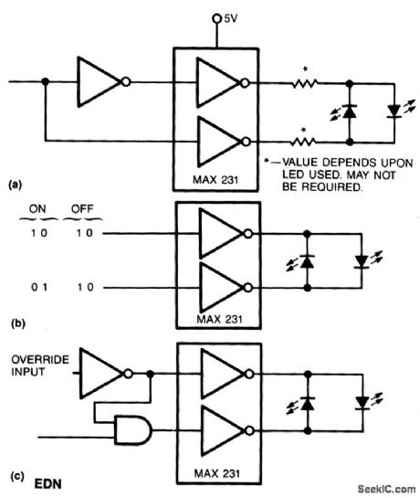
Use a pair of Maxim's 5V-powered MAX231 RS-232C transmitters as drivers to obtain a 2-color LED. The transmitters require only a singleended, 5-V input to generate ±10 V internally.Their outputs are short-circuit-proof and can supply as much as 10 mA-enough to drive most LEDs.Depending on which LED you select, their currentlimiting feature might also eliminate the need for external series resistors. Using the simple circuits, you can implement a variety of functions.
(View)
View full Circuit Diagram | Comments | Reading(870)
LOW_LEVEL_CMOS_COIVTROL
Published:2009/7/7 2:16:00 Author:May

Low-level output of CMOS buffer turns on DC motor through Q1 and 20-A Darlington power transistor Q2.-A. Pshaenich,” Interface Techniques Between Industrial Logic and Power Devices,” Motorola, Phoenix, AZ, 1975, AN-712A, p 18. (View)
View full Circuit Diagram | Comments | Reading(926)
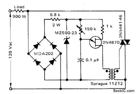
DISCO_STROBE_LIGHT
Published:2009/7/6 20:08:00 Author:May
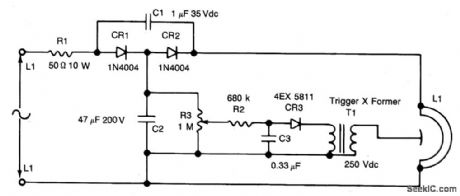
This circuit uses a voltage doubler CR1 and CR2 to obtain about 280 V dc across C1. C2 and R3 form a voltage divider to obtain a dc voltage to change C3 thru R2. When CR3 fires, a high voltage is generated in T1, firing L1.
(View)
View full Circuit Diagram | Comments | Reading(1399)
LAMP_FLASHER
Published:2009/7/6 9:06:00 Author:May
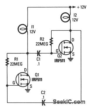
The circuit is built around two power FETs, which are configured as a simple astable multivibra-tor to alternately switch the two lamps on and off. The rc values given sets the flash rate to about 1/3 Hz. By varying either the resistor or capacitor values, almost any flash rate can be obtained. Increase either C1 and C2, or R1 and R2, and the flash rate slows. Decrease them and the rate increases. (View)
View full Circuit Diagram | Comments | Reading(847)
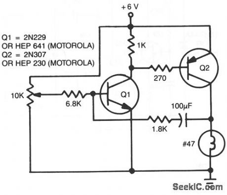
MINIMUM_COMPONENT_FLASHER
Published:2009/7/6 9:05:00 Author:May
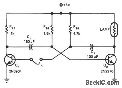
Opening SA, changes the indicator lamp from flashing to steady-lit condition. The 6-V incandes-cent lamp on the collector of Q2 requires about 0.3 A. A 1-KΩ load resistor limits Q1's collector cur-rent to about 6 mA. The circuit is, therefore, asym-metrical with respect to the on currents of the transistors, allowing use of a much smaller transistor for Q1 than for Q2. (View)
View full Circuit Diagram | Comments | Reading(854)
TRANSISTOR_FLASHER
Published:2009/7/6 9:04:00 Author:May
This astable multivibrator uses incandescentlamps In place of collector load resistors. The lamps flash on and off alternately. (View)
View full Circuit Diagram | Comments | Reading(1047)
ALTERNATING_LED_FLASHER_1
Published:2009/7/6 9:02:00 Author:May
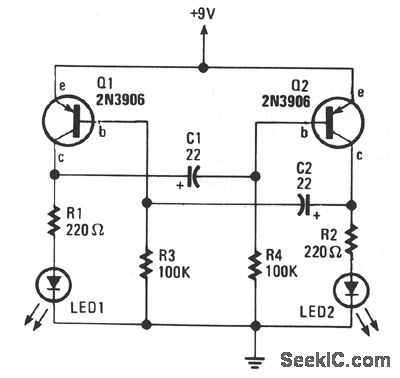
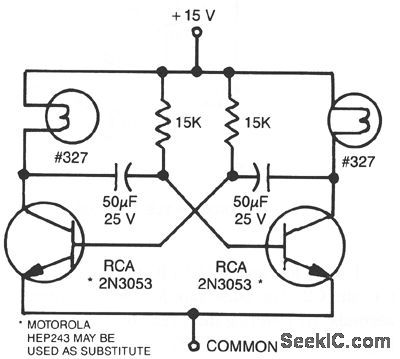
The alternating LED flasher is simply a two-transistor oscillator with LEDs connected to the collector of each transistor, so that they light in time with the circuit's oscillations. (View)
View full Circuit Diagram | Comments | Reading(1860)
60_W_FLASHING_LIGHT
Published:2009/7/6 9:01:00 Author:May
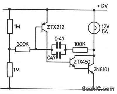
The 2N6101 transistor should be mounted on a small heatsink. The 300-KΩ resistor controls the off period and might need to be adjusted if transistor gains are high. The 100-KΩ resistor controls the on period. (View)
View full Circuit Diagram | Comments | Reading(901)
ALTERNATING_LED_FLASHER
Published:2009/7/6 8:58:00 Author:May

The timing components are R1, R2, and Ct. C1 is a bypass capacitor used to reduce the effects of noise. At start-up, the voltage across Ct is less than the trigger level voltage (1/3 VDD), causing the timer to be triggered via pin 2. The output of the timer at pin 3 increases, turning LED1 off, LED2 on, the discharge transistor at pin 7 off, and allowing Ct to charge through resistors R1 and R2. When capacitor Ct charges to the upper threshold voltage (2/3 VDD), the flip-flop is reset and the output at pin 3 decreases. LED1 is turned on, LED2 is turned off, and capacitor Ct discharges through resistor R2 and the discharge transistor. When the voltage at pin 2 reaches 1/3 VDD, the lower threshold or trigger level, the timer trig-gers again and the cycle is repeated.The totem-pole output at pin 3 is a square wave with a duty cycle of about 50%. The output alternately turns on each LED at slightly less than one blink per second. If the unit is battery operated, the TLC555 uses minimum current to produce this function. With a 9-V battery, the circuit draws 5 mA (noload) and 15 mA when turning on an LED. Most of the on current is for the LED. (View)
View full Circuit Diagram | Comments | Reading(884)
INCANDESCENT_LIGHT_FLASHER
Published:2009/7/6 8:50:00 Author:May
View full Circuit Diagram | Comments | Reading(1024)
SINGLE_LAMP_FLASHER
Published:2009/7/6 8:45:00 Author:May
The flash rate is controlled by a complementary multivibrator consisting of an npn and a pnptransistor. (View)
View full Circuit Diagram | Comments | Reading(911)
THREE_YEAR_LED_FLASHER
Published:2009/7/6 8:39:00 Author:May
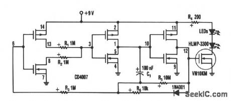
Inserting two 1-MΩ resistors, R1 and R2, in the output stage of one of the circuit's inverters limits the current needed by the oscillator to no more than a few μA. This circuit includes a CD4007 package, which has three CMOS inverters. It forms a standard three-inverter oscillator. Resistors R1 and R2, in series with separate drains on inverter pins 8 and 13, limit the oscillator's supply current. Capacitor C1 and resis-tors R5 set the off time of the oscillator, C1; R6 sets the on time. A VN10KM small-power FET, current-limited by R4, drives two HLMP-3300 LEDs. The LEDs consume about 20 mA for 1 ms. Their average current determines battery life. Since the LEDs in the circuit flash at 1 Hz, the average current drain is about 1/1000 of 20 mA, or 20 μa. A 9-V battery should last about three years at the current drain-essen-tially the shelf life of an alkaline battery. (View)
View full Circuit Diagram | Comments | Reading(1675)
RING_AROUND_LED_FLASHER
Published:2009/7/6 8:35:00 Author:May

When power is first turned on, two of the LEDs are on and the other two remain off until the timing cycle reverses. The LEDs flash in pairs, but by pressing and holding S1 closed until only one of the LEDs is on, and then releasing it, the four LEDs can be made to flash in sequential order. The number of LEDs flashing in a sequential ring can be easily increased to eight by adding another 4001 quad NOR gate. Just repeat the circuit and connect the additional circuit in series with the first-input to output-as an extension of the first circuit. When power is connected to the eight-LED flasher circuit, four LEDs will turn on at once and then flash off as the four remaining LEDs come on. As before, just press S1 and hold closed until all but one LED turns off; then the LEDs will begin their sequential march in a circle. You can connect as many circuits in series as you like. (View)
View full Circuit Diagram | Comments | Reading(1118)
BRIDGE_BALANCE_INDICATOR
Published:2009/7/6 4:42:00 Author:May
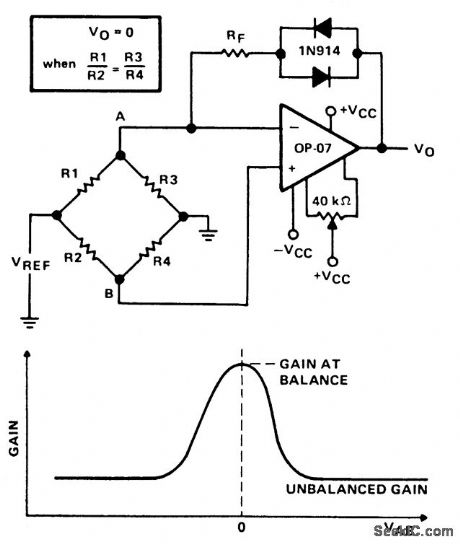
Indicator provides an accurate comparison of two voltages by indicating their degree of balance (or imbalance). Detecting small variations near the null point is difficult with the basic Wheatstone bridge alone. Amplification of voltage differences near the null point will improve circuit accuracy and ease of use.The 1N914 diodes in the feedback loop result in high sensitivity near the point of balance (R1/R2=R3/R4). When the bridge is unbalanced the amplifier's closed-loop gain is approximately RF/r, where r is the parallel equivalent of R1 and R3. The resulting gain equation is G = RF(1/R1+1/R3). During an unbalanced condition the voltage at point A is different from that at point B. This difference voltage (VAB), amplified by the gain factor G, appears as an output voltage, As the bridge approaches a balanced condition (R1/R2 = R3/R4), VAB approaches zero. As VAB approaches zero the 1N914 diodes in the feedback loop lose their forward bias and their resistance increases, causing the total feedback resistance to increase. This increases circuit gain and accuracy in detecting a balanced condition. The figure shows the effect of approaching balance on circuit gain. The visual indicator used at the output of the OP-07 could be a sensitive voltmeter or oscilloscope. (View)
View full Circuit Diagram | Comments | Reading(1361)
50_Mb_s_FIBER_OPTIC_LED_DRIVER_
Published:2009/7/6 4:35:00 Author:May
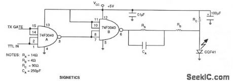
The pull-up transistor of the totem-pole output is used to turn on the LED and the pull-down transistor is used to turn off the LED. The lower impedance and higher current handling capability of the saturated pull-down transistor is used as an effective method of transferring the charge from the LED's anode to ground as its dynamic resistance increases during turn-off. The slightly higher output impedance of the pull-up stage ensures that the LED is not over peaked during the less difficult turn-on transition. This asymmetric current handling capability of the output stage with its variable impedance substantially reduces the pulse-width distortion and long-tai]ed response. As the signal propagates through two NAND gates, each transition passes through the high-to-low and low-to-high transition once, normalizing the total propagation delay through the circuit. (View)
View full Circuit Diagram | Comments | Reading(858)
| Pages:46/72 At 204142434445464748495051525354555657585960Under 20 |
Circuit Categories
power supply circuit
Amplifier Circuit
Basic Circuit
LED and Light Circuit
Sensor Circuit
Signal Processing
Electrical Equipment Circuit
Control Circuit
Remote Control Circuit
A/D-D/A Converter Circuit
Audio Circuit
Measuring and Test Circuit
Communication Circuit
Computer-Related Circuit
555 Circuit
Automotive Circuit
Repairing Circuit