
Circuit Diagram
Index 1775
Projectile Speed Test Circuit Diagram
Published:2011/5/20 20:57:00 Author:leo | Keyword: Projectile Speed Test Circuit Diagram, HCT4060, 4096, MOSFET
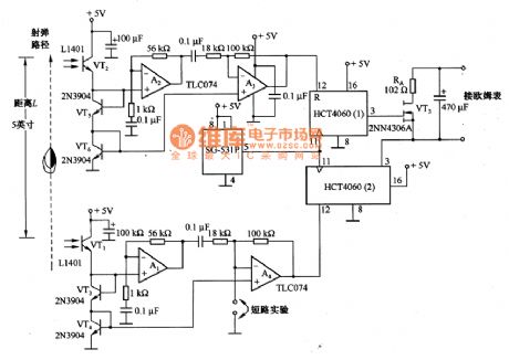
The picture shows a projectile speed test circuit. In the circuit, VT1 and VT2 are phototransistors. Projectile speed begins to be tested when the projectile passes through VT1. When projectile shades VT1, it can be considered as adding 500μV pulse to non-inverting input of A1. The pulse is amplified and reversed through A1 and A4 and offer starting impulse for HCT4060(2)-the 14 bits asynchronous counter. After this, the path of projectile is calculated again from zero and the speed will be calculated by 250ns resolution. At the same time, when projectile reaches VT2, it begins to test HCT4060(1) to test the destination of the projectile. (View)
View full Circuit Diagram | Comments | Reading(1374)
555 stimulated ozone generator circuit
Published:2011/5/23 8:53:00 Author:TaoXi | Keyword: stimulated, ozone generator
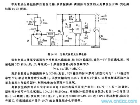
This ozone generator is composed of the step-down rectifier circuit, the multivibrator source and the ozone generating piece. The circuit is as shown in figure 16-37.
The power supply is composed of the step-down transformer and the full-bridge rectifier circuit, after the voltage stabilization of the 7809, the power supply supplies the +9V DC voltage. The multivibrator is composed of the time base circuit 555 and the R3,R4,C4, the oscillation frequency is f=1.44/(R3+2R4)C4.
The figure parameter's oscillation frequency is about 30 kHz. The 555 output pulse sequence (the duty ratio is about 1:1) drives the high-frequency pulse transformer T1 through the power tube VT1, the bubprime output voltage is about 3000V. This kind of high-frequency high-voltage pulse adds to the ozone generating pottery to produce the ozone by the corona discharging principle.
(View)
View full Circuit Diagram | Comments | Reading(2321)
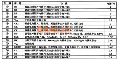
VOGUE 9866-1 Communication single-chip integrated circuit diagram
Published:2011/6/1 22:26:00 Author:leo | Keyword: VOGUE 9866-1 Communication single-chip integrated circuit diagram
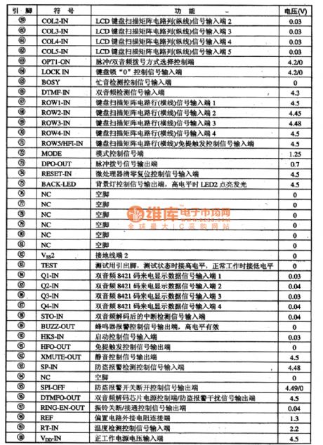
VOGUE 9866-1 is a type of communication single-chip integrated circuit which is always used in caller ID telephone.
1. Function Features:The integrated circuit VOGUE 9866-1 consists of FSK decoder, duel-tone signals generator, LCD gate driver, keyboard switch coder, keyboard lock 0 controller, busy tone detector, duel-tone 8421 interface, on-hook, burglar alarm, pulse signal generator, buzzer warning controller, mute controller, ringing on/off controller, temperature test controller, mode controller and other circuits. It is usually used together with DTMF caller ID integrated circuit to finish the DTMF caller ID function.
2. Pin functions and data:The integrated circuit VOGUE 9866-1 adopts 100-pin soft package whose chip is directly packed in the LCD. Its pin functions and data are shown in the picture 1-1-1. (View)
View full Circuit Diagram | Comments | Reading(978)
The circuit diagram of preamplifier serving the electric motor drive circuit
Published:2011/6/1 22:31:00 Author:leo | Keyword: The circuit diagram of preamplifier serving the electric motor drive circuit, MC1437
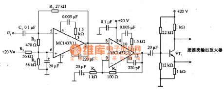
Picture 1 shows a preamplifier that serves the electric motor drive circuit. In this circuit, 90° phase shift adopts differential coefficient circuit with operational amplifier MC1437 (1). It is connected to in-phase amplifier MC1437 (2) with the voltage plus of 40 dB. Feedback resistance R1 and input capacitance C1 can make up of differential circuit. R3 and R4 are used to set DC operating point of operational amplifier. And the operating point is set in the 1/2 of the voltage of power supply. The gain of differential circuit increases by the frequency. Therefore, the circuit may develop into high-frequency section and it needs to limit bandwidth. The single-ended output of MC1437 (2) passes VT1 and becomes two ways signals in order to drive sh-pull (PP) output amplifier. (View)
View full Circuit Diagram | Comments | Reading(699)
555 multi-purpose electronic treatment health device circuit
Published:2011/5/23 22:18:00 Author:TaoXi | Keyword: multi-purpose, electronic, treatment, health device
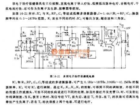
As the figure 16-21 shows, the low-frequency multivibrator is composed of the IC1 and R1,RP1,C1, f=1.44/(R1+RP1)C1, the oscillation frequency is in the range of 0.5~187Hz. If K1 is in the different positions, IC1 can output the square wave, sawtooth wave and the delta wave.
The multivibrator is composed of the IC2 and R3,RP2,C3,C4, this multivibrator produces the oscillation frequencies of 0.5Hz~187Hz and 106Hz~41.2kHz. IC1 can modulate the IC2. By controling the K2,K3,K4 and K5, we can get the different modulation waves. If you connect the infrared glowing tube D5 to this circuit, this circuit can output the infrared modulation wave. When the K6 is in the position of 2 , the signal is amplified by VT2 and is boosted by T2, the secondary stage of T2 can produce the anion with the high-pressure corona method.
(View)
View full Circuit Diagram | Comments | Reading(759)
555 frequency and duty ratio adjustable electronic therapeutic equipment circuit
Published:2011/5/24 1:29:00 Author:TaoXi | Keyword: frequency, duty ratio, adjustable, electronic therapeutic
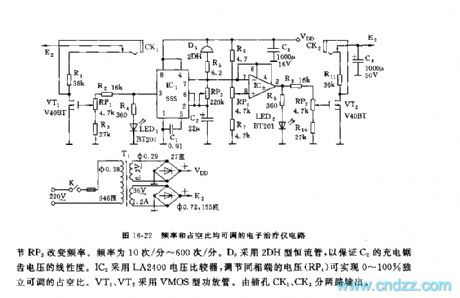
As the figure 16-22 shows, the electronic therapeutic equipment is composed of the pulse generator, the voltage comparator, the amplifier stage and the power supply.
The step-down rectifier circuit can produce the voltage of VDD=+8V and E2=+40V as the electronic therapeutic equipment's power supply. The astable multivibrator is composed of the IC1, R5,RP3,C2 and the constant-current tube D3, the oscillation frequency f=1.44/(R5+RP3)C2, you can change the frequency by adjusting RP3. D3 uses the 2DH type constant-current tube to guarantee the linearity of C2's charging sawtooth voltage. IC2 uses the LA2400 voltage comparator. VT1 and VT2 uses the VMOS type power amplifier tube. The voltage is output by the two channels of Jacks CK1 and CK2.
(View)
View full Circuit Diagram | Comments | Reading(780)
555 DGK—45L disinfection cabinet electronic control circuit
Published:2011/5/25 3:09:00 Author:TaoXi | Keyword: 555, disinfection cabinet, electronic control
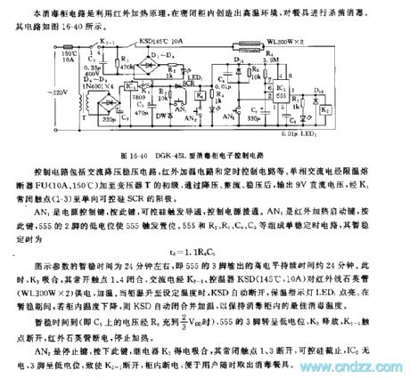
The control circuit is composed of the AC step-down voltage stabilization circuit, the infrared heating circuit and the timing control circuit.etc. The single phase alternating current adds to the primary stage of the transformer T through the temperature limit fuse FU(10A, 150℃), after the function of step-down, rectification and voltage stabilization, the transformer T outputs the 9V DC voltage, this voltage adds to the single phase SCR's positive electrode through K1's normal closing contacts (1-3).
AN1 is the power control button, you can conduct the SCR and control the connection of the power supply by pressing this button. AN3 is the infrared heating start button, if you press this button, the low electric potential of the 555 pin-2 sets the 555. The monostable timing circuit is composed of the 555 and R5,R6,C4,C5, the Temporary stabilization time td=1.1R6C5.
(View)
View full Circuit Diagram | Comments | Reading(535)
The push-pull power amplifier circuit formed by MOSFET
Published:2011/6/9 3:02:00 Author:leo | Keyword: The push-pull power amplifier circuit formed by MOSFET
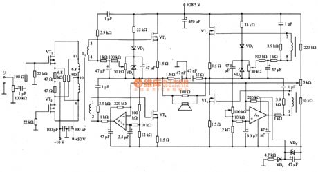
The picture 1 shows a push-pull power amplifier circuit formed by MOSFET. VT1 and VT2 form the propel circuit, which uses transformer T1 to get the same output value but different polarity signals. And the signals are driven separately by the power output ports formed by VT3 and VT4 (VT5 and VT6). In order to increase output power, when the operating power is 1 kHz, the minimum distortion is 0.25%. The voltage gain of median frequency period is 31.5 dB.When voltage gain is -3dB, the bandwidth is narrow, which is 11 kHz to 16.8 kHz. When input port is short or cut off, noise voltage is 0.22 mV. So it has excellent performance.
(View)
View full Circuit Diagram | Comments | Reading(2948)
555 patient faint language alarm box circuit
Published:2011/5/25 3:47:00 Author:TaoXi | Keyword: 555, patient, faint, language alarm, box
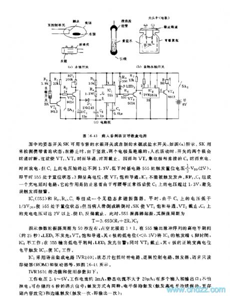
The language alarm box is composed of the posture switch, the oscillating circuit and the language alarm circuit, as the figure 16-43 shows.
The astable multivibrator is composed of the IC1(555) and R3,R4,C2.etc. In the peace time, C2's voltage is lower than 1/3VDD, this makes the 555 in the setting state; when the patient falls down, SK makes the VT1 in the saturated conduction state, VT2 cuts off, C2's charging voltage is higher than 2V to make the D1 to cuts off.
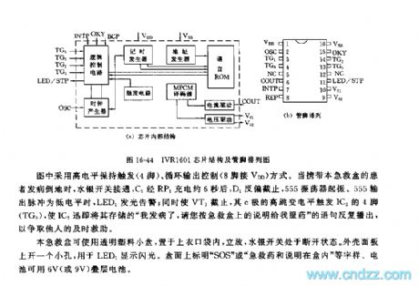
The IC2 uses the language integrated circuit IVR1601, this chip is composed of the clock circuit, the logic control circuit, the trigger circuit, the language read-only memory (ROM) and the driver.etc.
(View)
View full Circuit Diagram | Comments | Reading(587)
555 alpha/theta meditation device circuit
Published:2011/5/25 4:03:00 Author:TaoXi | Keyword: 555, alpha, theta, meditation device
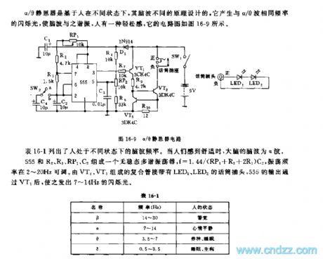
The design principle of the alpha/theta meditation device depends on human have different brain waves in different conditions, it can produce the flashing light which has the same frequency with the alpha/theta wave to make the brain wave in the resonance oscillation state, so people feel good, the circuit is as shown in figure 16-9.
The table 16-1 shows the brain wave frequencies of different conditions. When you feel good, the brain wave frequency is the alpha wave.
The astable multivibrator is composed of the 555 and R2,R3,RP1,C2, f=1.44/(RP1+R2+2R3)C2, the oscillation frequency is between 2~20Hz. The output of 555 gets through the VT1, and makes the VT1 issues the 7-14Hz flashing light.
(View)
View full Circuit Diagram | Comments | Reading(2438)
555 home appliance timing power-off controller circuit
Published:2011/6/7 0:56:00 Author:TaoXi | Keyword: 555, home appliance, timing, power-off, controller
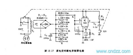
As the figure 15-17 shows, the timing power-off control circuit is composed of the step-down rectifier circuit and the timing circuit.etc. When you press the button switch AN, the electric potential of 555's pin-2 is lower than the trigger electrical level 1/3VDD, so the 555 circuit turns, pin-3 outputs the high electrical level, the relay J closes and the J1-1 contact point closes too, the socket gets the power, the circuit starts timing at this time. The capacitance C is charged through R, when the voltage of C is higher than the threshold level 2/3VDD, 555 circuit resets, pin-3 has the low electrical level, J releases and J1-1 cuts off, the appliance has no power.
(View)
View full Circuit Diagram | Comments | Reading(595)
555 household appliance products long timing circuit
Published:2011/6/7 1:40:00 Author:TaoXi | Keyword: 555, household appliance, products, long timing
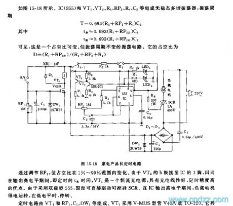
As the figure 15-18 shows, the astable multivibrator is composed of the IC(555) and VT1, VT2, R1, RP2, R4, C2, the oscillation period T=0.693(R1+RP2+R4)C2.
Because the b electrode of VT2 connects to the pin-3 of IC, so when pin-3 outputs the high electrical level, VT1 is a constant-current charging source, it has good charging linear and timing precision. Because it uses the bipolar type 555, so it can drive the SCR directly. When the IC outputs the high electrical level, the load gets power to work, when the IC outputs the low electrical level, the load has no power to work.
The timing circuit is composed of the VT3 and RP1, C1, DW1.etc. The VT3 uses the VCMOS type tube V40A or TO-220.
(View)
View full Circuit Diagram | Comments | Reading(471)
555 flowerpot deaquation alarm circuit
Published:2011/6/7 2:00:00 Author:TaoXi | Keyword: 555, flowerpot, deaquation, alarm
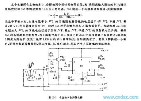
As the figure 15-5 shows, the low-frequency multivibrator is composed of the 555, the oscillation frequency f=1.44/(R5+2R6)C.
When the pot does not dry, the resistivity of the soil is small, the voltage between the VT1's G pole and the circuit's ground voltage is nearly 0V, VT1 conducts, VT2 cuts off, so the voltage of the VT2's emitter is 0V. At this time the 555 is in the non-trigger state, pin-3 has the low electrical level. When the soil is dry, the resistance between A and B increases, the electric potential of the VT1's G pole is nearly the negative pressure, VT1 cuts off, VT2 conducts, VT2's emitter potential increases.
According to the features of the 555 time-based circuit, when the electric potential of pin-4 is higher than 0.4V, the 555 might be in the oscillation condition, the output port pin-3 has the high electrical level, and the LED's frequency is 1Hz.
(View)
View full Circuit Diagram | Comments | Reading(568)
555 household time-limit alarm circuit
Published:2011/6/7 2:25:00 Author:TaoXi | Keyword: 555, household, time-limit, alarm
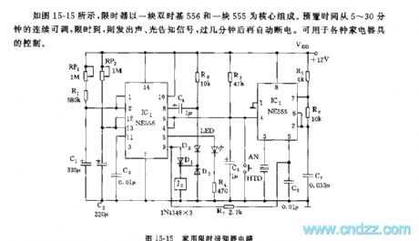
As the figure 15-15 shows, the preset timer uses one piece of dual time-base 556 and one piece of 555 as the core. The preset time is 5 to 30 minutes, when the time is up, this circuit will send out the sound-light alarm signal, and after a few minutes, this circuit will cut off the power automaticly. It can be used to control all sorts of home appliances.
The RP1, R1, C1 and 1/2 556 can be used in the 5 to 30 minutes boot timing. When the power supply opens, the C1's electric potential can not be mutated, so the timing circuit sets and the timeing starts, the timing time td1=1.1(RP1+R1)C1, you can change the timing length by adjusting RP1. The monostable delay circuit is composed of the RP2, C2 and another half of 556, the delay time depends on the time constants of RP2 and C2.
(View)
View full Circuit Diagram | Comments | Reading(900)
555 hand-wave stop noising electric clock circuit
Published:2011/6/7 3:35:00 Author:TaoXi | Keyword: 555, hand-wave, stop noising, electric clock
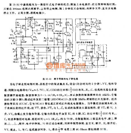
When the electric clock goes to the alarm moment, the contact point K1 of the original movement closes (the closing time is about 2 minutes), VT5 conducts, the additional circuit gets the power. The astable multivibrator which is composed of the left part (1/2 556) of the IC1(556) and the R9, R10, C7 starts oscillation, the oscillation frequency f=1.44/(R9+2R10)C7, the parameters of the figure has the oscillation frequency of 38kHz, it outputs the square wave to drive the infrared emitting diode LED(HG411).
When the hand is near the probe, the infrared ray which is reflected by the hand is received by the VT1, then this infrared ray is selected by the frequency-selecting amplifier which is composed of the VT2 and L1, C3 to rise the VT3's Vc.
(View)
View full Circuit Diagram | Comments | Reading(649)
888 safety box and refrigerator door-opening over-time sound alarm circuit
Published:2011/6/7 3:53:00 Author:TaoXi | Keyword: 888, safety box, refrigerator, door-opening, over-time, sound alarm
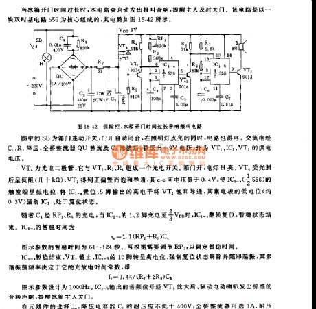
The SB in the figure is the refrigerator door linkage switch, when the door opens, the SB automatically shuts off, when the light turns on, the circuit gets power. The alternating current is reduced by C1 and R1, then it is rectified by the full bridge rectifier QU and is filtered by C2 to output the +9V voltage.
The VT4 is the photoelectric diode, the photoelectric switch is composed of the VT1, R3, R4 and the VT4. When the refrigerator door is opening, the light H turns on. VT4 has the low resistance because of the illumination (tens of thousands of ohms), VT1 gets the positive bias to conduct, the voltage between c and e is lower than 0.4V to make the IC1-n(1/2 556)'s trigger port has low electric potential, if you set the IC1-n, the pin-5 outputs the high electrical level to conduct the VT2.
(View)
View full Circuit Diagram | Comments | Reading(596)
The audio frequency power amplifier with 40W to 60 W output power and formed by MOSFET
Published:2011/6/10 21:09:00 Author:leo | Keyword: The audio frequency power amplifier with 40W to 60 W output power and formed by MOSFET
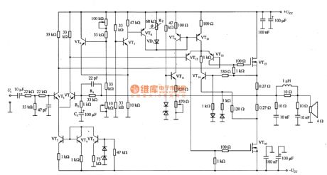
The picture 1 shows a audio frequency power amplifier circuit diagram. It is made up of MOSFET with the output power of 40 to 160 W. In this circuit, the DC current feedback between power output stages to preamplifier stage is decided by the value of R1, while the AC current feedback is decided by the resistance value and capability of C1. The basic amplifying circuit is formed by series connecting the two stages differential amplifiers of VT1, VT2 and VT12 and VT13. The operating point of VT1 and VT2 is decided by constant current circuit VT3, while it is the same condition to VT12 and VT13. VT6, VT7, VT8 and thermistor RT form temperature protection circuit. VT14 forms the over current protection circuit. When the current value of output power MOSFET is stronger than the set value, VT14 is connected while VT12 and VT13 push the current to be weakless, and VT15 and VT16 is cut off. Therefore, all processes reach the final result of protecting the MOSFET. (View)
View full Circuit Diagram | Comments | Reading(3352)
M62438-dual channel SUR solution circuit
Published:2011/6/10 21:24:00 Author:leo | Keyword: M62438-dual channel SUR solution circuit
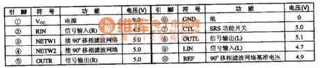
M62438 is the integrated circuit of the dual-channel analog SUR solution, which is widely used in audio devices and audio system of the advanced big screen color TV. It is produced by Mitsubishi in Japan.
1.Function features:M62438 contains two 90 angel phase-moving filter system, SRS function switch control circuit, basic power supply circuit of 90 angle phase-moving filter system, and other related circuits.
2.Pin function and dataM62438 adopts 10-pin package methods. Functions of all pins and related data are shown in the picture. (View)
View full Circuit Diagram | Comments | Reading(680)
555 two-tone electronic doorbell circuit (1)
Published:2011/6/7 4:08:00 Author:TaoXi | Keyword: 555, two-tone, electronic doorbell
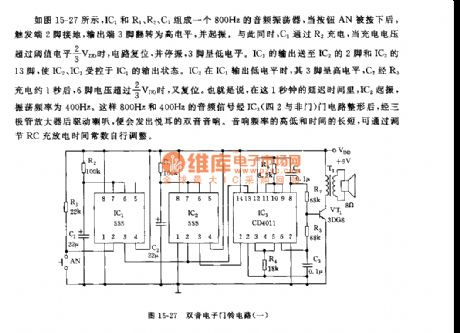
As the figure 15-27 shows, the 800Hz audio oscillator is composed of the IC1, R1, R2, C1, when you press the button AN, the trigger port pin-2 connects with the ground, the output port pin-3 has the high electrical level and starts oscillation. At the same time, the C1 is charged through R2, when the charging voltage is higher than the threshold level 2/3VDD, the circuit resets and stops oscillation, pin-3 has the low electrical level. IC1's output adds to the IC2's pin-2 and IC3's pin-13 to make the IC2 and IC3 controlled by the IC1's output state. When the IC1 outputs the low electrical level, pin-3 of IC2 has the high electrical level, C2 is charged for 1 second through R3, pin-6's voltage is higher than 2/3VDD, the circuit resets again. That is to say during the 1 second delay time, the IC2 starts oscillation, the oscillation frequency is 400Hz.
(View)
View full Circuit Diagram | Comments | Reading(1024)
The microcomputer dialing circuit UM-915-3
Published:2011/6/10 21:32:00 Author:leo | Keyword: The microcomputer dialing circuit UM-915-3
UM-915-3 is a microcomputer dialing circuit which is applied in all kinds of telephone.
1.Function features:Integrated circuit UM-915-3 contains a pulse dialing signal processing circuit and key switch code circuit and other circuits.
2.Pin function:Functions of all pins and related data of UM-915-3 are shown in the picture. (View)
View full Circuit Diagram | Comments | Reading(659)
| Pages:1775/2234 At 2017611762176317641765176617671768176917701771177217731774177517761777177817791780Under 20 |
Circuit Categories
power supply circuit
Amplifier Circuit
Basic Circuit
LED and Light Circuit
Sensor Circuit
Signal Processing
Electrical Equipment Circuit
Control Circuit
Remote Control Circuit
A/D-D/A Converter Circuit
Audio Circuit
Measuring and Test Circuit
Communication Circuit
Computer-Related Circuit
555 Circuit
Automotive Circuit
Repairing Circuit