
Circuit Diagram
Index 1764
AC Voltage Regulator Thirteen
Published:2011/6/3 8:33:00 Author:Michel | Keyword: AC, Voltage Regulator, Thirteen
The AC voltage regulator introduced in the example uses servo-type control circuit.It has good dependability and wide adjustable range.
Circuit's Wrok Principle
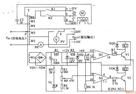
The circuit is composed of voltage stabilizing circuit,voltage test control circuit and voltage regulation output circuit and it is showed as the picture 5-52.The voltage stabilizing circuit consists of self-coupling transformer,T,communication diode VD1-VD4,filter capacitor CT,current-limitting resistor R1,R2 and voltage regulation diode VS1,VS2.
The voltage test control circuit is composed of R3-R9,diode VD5,VD6,LED VL,relay K1,K2,potentiometer RP,transistor V1,V2 and operational amplifier IC(N1,N2). (View)
View full Circuit Diagram | Comments | Reading(2895)
Switch D. C. Regulated Power Supply Two
Published:2011/6/3 4:39:00 Author:Michel | Keyword: Switch, D. C., Regulated Power Supply, Two
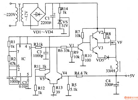
This example introduces the switch D. C. regulated power supply circuit of buck-mode +5V series.It is composed of power supply circuit,impulsator,voltage sampling or pulse width modulation circuit, buffering driver circuit and it is showed as the picture 5-38.The input converting circuit consists of mains transformer,T,commutation diode VD1-VD4,filter capacitor C1,current-limiting resistor and voltage regulator diode VS.The impulsator consists of time-base integrated circuit IC,resistor,R1,R2 and capacitor,C2,C5.The voltage sampling or pulse width modulation circuit is composed of capacitor,C3,resistor,R3-R5,R11-R13 and transistor V4 and V5. (View)
View full Circuit Diagram | Comments | Reading(2850)
Switch D. C. Regulated Power Supply One
Published:2011/6/3 3:52:00 Author:Michel | Keyword: Switch , D. C., Regulated Power Supply, One
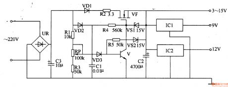
The switch D. C. regulated power supply circuit introduced in the example can supply 3-15V D.C. voltage and its maximum current is 150mA,which meet the miniaturized electronics' power supply.
Work's Principle of the CircuitThe switch D. C. regulated power supply circuit is composed of rectifying and wave-filtering circuit,switch control circuit and voltage regulator circuit and it is showed as the picture 5-37.
The rectifying and wave-filtering bridge,UR,commutation diode,VD1,VD2 and filter capacitor,C1 and C3.The switch control circuit consists of resistor,R2 and R4,voltage regulator diode,VS1 and field effect transistor,VF.The voltage regulator circuit is composed of resistor R1,R3,R5,voltage regulator diode VS2,transistor,V,diode,VD3,filter capacitor C2 and three-terminal integrated regulator IC1 and IC2.
(View)
View full Circuit Diagram | Comments | Reading(1215)
D. C. Regulated Power Supply of High Voltage One
Published:2011/6/3 1:02:00 Author:Michel | Keyword: High Voltage, D. C., Regulated Power Supply, One
.
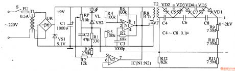
The high voltage D. C. regulated power supply introduced in the example has the simple circuit and high work efficiency and the output circuit voltage can be regulated constantly between 0-2V and it can be used as high voltage power of electronic components measure, science and education experiment.
Work's Principle of the Circuit
The high voltage D. C. regulated power supply circuit consists of mains input circuit,multivibrator type oscillator,voltage adjustment and stabilization circuit,voltage booster circuit and it is showed as the picture 5-35.The mains input circuit is composed of mains switch,S,fuse,FU,mains transformer,T,rectifier bridge,UR,voltage regulator diode,VS, and filter capacitor,C1.The multivibrator type oscillator circuit consists of operational amplifier IC(N1and N2),N1,resistor,R4-R7and capacitor,C3. (View)
View full Circuit Diagram | Comments | Reading(5491)
Numerical Control D. C. Regulated Power Supply Fifteen
Published:2011/6/2 12:07:00 Author:Michel | Keyword: Numerical Control, D. C., Regulated Power Supply, Fifteen
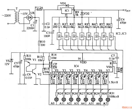
The numerical control D. C. power-supply circuits-fixed introduced in the example uses metal touch button ,digital IC and electron switch IC to converse the magnitude of output voltage.Compared to D. C. regualted power-supply cf traditional mechnical range switch,it has the advantage of lowbreakdown and convenient operation.
Work's Principle of the Circuit
The numerical control D. C. power-supply circuits-fixed is composed of mains circuit,free-running multivibrator,counting distributor,analog switching circuit and control circuit and it is showed as the picture 5-34.The mains circuit consists of mains transformer,T,rectifier bridge,UR,capacitor,C1-C5,resistor,R9,R10,diode,VD1,VD2,three-terminal integrated regulator,IC1 and zener diode,VS. (View)
View full Circuit Diagram | Comments | Reading(2004)
Automatic Switching of AC and DC Input Circuit
Published:2011/5/17 6:01:00 Author:Joyce | Keyword: Automatic Switching, of AC and DC, Input
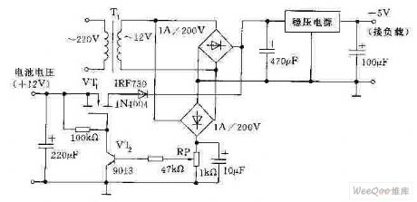
The following graph is the automatic switching of AC and DC circuit .After being depressurized by transformer T1, the electric supply will be output after rectifying, filtering and voltage stabilization to make the load work. Meanwhile, another route will go to the base of VT2 after going through a direct voltage produced by rectifying and filtering and being divided by RP. So VT2 will break over and VT1 will cut off. When the electric supply breaks off, VT2 will cut off and MOSFET VT1 will break over. Storage battery will supply the voltage-stabilizing circuit through VT1 andoutput stable direct voltage for the load. Due to the application of MOSFET to conduct fast electronic switching, this circuit has achieved the purpose of uninterrupted power supply. (View)
View full Circuit Diagram | Comments | Reading(701)
Bi-directional Thyristor-composed AC Voltage Regulation Circuit
Published:2011/5/17 8:07:00 Author:Joyce | Keyword: Bi-directional Thyristor-composed, AC, Voltage Regulation
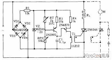
As shown in the graph below, the circuit uses to control heaterload RL (resistance wire). The trigger circuit uses UJT relaxation oscillators. It issupplied after the AC power supply is rectified via rectifier bridge and sliced into trapezoidal DC via resistance R1 and stabilivolt VZ .Output of SJU goes to the bi-directional thyristor door gate circuit after being coupled by pulse transformer. If you want to control the speed of DC motor M,you can connect the bi-directional thyristor and the motor in parallel according to the dotted line in the graph. In this way, it can absorb the overvoltage of the bidirectional thyristor, which is caused by the discharge of inductive load.
(View)
View full Circuit Diagram | Comments | Reading(885)
MAX1916 Output Parallel Connection Circuit
Published:2011/5/17 5:59:00 Author:Joyce | Keyword: MAX1916, Output, Parallel Connection
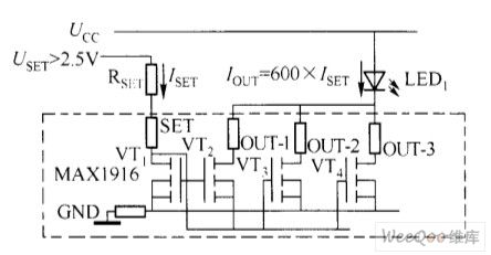
The drain source resistance of MAX1916 is set not to exceed 50Ω in the whole temperature range. A GaAsP - LED with a working current of 2mA guarantees the minimum voltage needed in proper function is UF + 1 00mV. Input voltage of 2.7 V can keep the working voltage of GaAsP - LED to2.7 V. In order to acquire lower differential pressure and higher output current, one can connect three ways of the output of MAX1916 in parallel to constitute a current source with 600A/A mirror coefficient . MAX1916 output parallel connection circuit is shown in the graph, and the drain source resistance is50/3 = 16.61 Ω (Max) if connected in this way. This kind of connectionallows the current of a single white light LED to reach 20mA above with 3V power supply,so as to meet current requirements in blacklight of products like portable mobile phones.Thevoltage source used to set the end-point current can be supplied by a main power with a strong load capacity alone,such as on mobile phones. USET can be supplied with a low noise + 2.8 V power source of RF circuit. If it is supplied directly by single lithium ion battery, MAX1916 can be applied to driveGaAsP - LED with relatively low forward voltage , and resort to other drive schemes for white light InGaN - LED with high forward voltage. Because when it is supplied by the lithium ion battery, as the discharge goes on,the input voltage may fail to reach the required bias voltage of the white light LED. (View)
View full Circuit Diagram | Comments | Reading(749)
Application Circuit of MAX1848
Published:2011/5/25 4:08:00 Author:Joyce | Keyword: Application Circuit of MAX1848
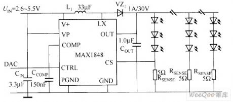
In applications requiring higher power, MAX1848 drive which is based on inductance can be used. MAX1848`s external circuit needs only a few components ,and the conversion efficiency can reach 88% if the output power is 800mW. MAXI848 integrates boost converter and current control circuit in 6 pins 50723 encapsulation.With electric current detection,it drives three groups of white light LED,andeach group includes 3 white light LED connected in parallel as shown in figure. The input voltage range of MAX1848 is 2.6 ~ 5.5 V. MAX1848 uses voltage feedback to adjust the current flowing through the white light LEDs, and smaller current detection resistance (5 Ω) helps to save power and keep high conversion efficiency. In the typical application circuit of MAX1848,the device parameters are: L1 = 33μH, CCOMP = 150nF, COUT = 1.0μF, RSENSE = 5Ω. The current of white light LED is decided by the control voltage: IOUT = UCTRL/( 18.33 xRSENSE).
The luminance of the white light LED can be regulated by DAC of CTRL pins or potentiometer bleeder circuit. And the controllable scope of voltage is + 250mV ~ + 5.5 V. To grounding the control pins shutoff the circuit. (View)
View full Circuit Diagram | Comments | Reading(597)
Driving White LED Circuit
Published:2011/5/18 9:45:00 Author:Joyce | Keyword: Driving White LED
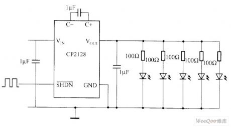
CP2128 is a step-up DC/DC converter of low noise and set frequency.If the input voltage isbetween 2.7 to 4.5 V,this device can produce 5v output voltage, and the current output can reach 100MA . Few external components make CP2128 a very suitable choice for small-sized applications in which battery is used as the power source . CP2128 charge pump can reduce fluctuation of output and input when full loaded and zero loaded. With overtemperature protection function, CP2128 can support continuous UOUT grounding. Because it has a high switching frequency, small ceramic capacitors are disposable.(1) the technical characteristics of CP2128The main technical characteristics CP2128 are as follows.①low noise and fixed frequency.②the output current: 100mA.③switching frequency: MHz 1.8.④fixed output voltage: 5 (1± 4%) V.⑤input voltage: 2.7 to 4.5 V.⑥automatic soft start to reduce inrush current.⑦no inductance.⑧when shut off.Icc<1μA(2) The typical application circuit of CP2128Application areas of CP2128 are: mobile phones, digital cameras, MP3, PDA, notebook computers, GPS receiver. The typical application circuit of CP2128 is as shown in the figure . (View)
View full Circuit Diagram | Comments | Reading(754)
Camera Nickel-cadmium Battery Discharger Circuit
Published:2011/5/17 8:04:00 Author:Joyce | Keyword: Camera, Nickel-cadmium Battery, Discharger
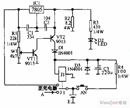
Camera Nickel-cadmium Battery Discharger Circuit is shown in the graph below.After preshing AN, J1 will actuate. At this time, because the voltage on the end of the battery is high, the potential,which has been divided by R1 W1 and then been injected into the baseVT is also high.Both VT1 and VT2 will breakover,and J1 will actuate to protect itself. The battery discharges mainly through IC1, R2, and the indicator light D2 will be on. When the battery voltage drops till it is insufficient for VT1 to breakover, J1 will discharge until its normally open contact disconnects. And when its normally close contact gets through charging circuit A,battery charging begins.
(View)
View full Circuit Diagram | Comments | Reading(1142)
Soft Start of the Power Supply Circuit Composed of L200
Published:2011/5/17 6:02:00 Author:Joyce | Keyword: Soft Start of, the Power Supply, Composed of L200
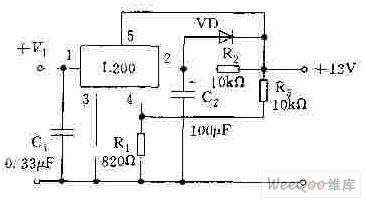
As shown in figure below,it starts using the maximum output current regulation and control of foot 2 of L200.In this way, C2 would prevent voltage jump of foot2 in starting up, and L200 remains the state ofsmallest output current. As foot5 charges C2 through R2,the output voltage of L200 would gradually increase.According to the component parameters in the graph, it takes 7s for the output voltage to reach the rated value.One also can delay the connection of L200 benchmark end foot 4 and R1 to achieve the purpose of soft start.
(View)
View full Circuit Diagram | Comments | Reading(1046)
Power Factor Measure Circuit
Published:2011/5/20 18:49:00 Author:leo | Keyword: Power Factor Measure Circuit, CD4066
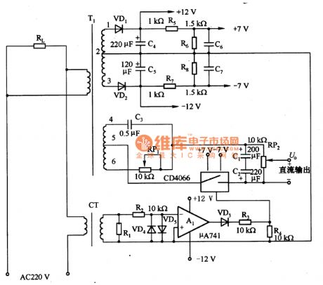
The picture is a power factor measure circuit. Power factor is used to show the phase relationship between voltage and electronic current. In the circuit, the voltage of T1 secondary 4 to 6 is used as the DC voltage sample and the secondary current of current transformer is used as the current sample. The current sample signal is amplified through A1 to control the analog switch CD4066 and takes effect with voltage sample, and then positive and negative DC voltages are generated.
(View)
View full Circuit Diagram | Comments | Reading(3670)
DC meter protection amplification circuit made by LM10 and others
Published:2011/5/20 18:52:00 Author:leo | Keyword: C meter protection amplification circuit, LM10
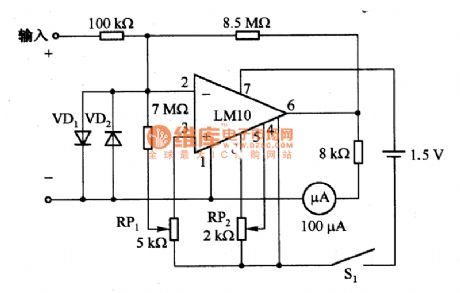
The picture 1 is a DC meter protection amplification circuit and is made up of LM10 and others. It is a kind of DC meter protection amplification circuit which needs to work in the temperature of 15 to 55 centigrade. The sensitivity of full scale is lOmV/l0nA. RP2 is used to set to zero. And the based voltage of setting zero is decided by the based voltage in the LM10 and does not affect by the voltage of power supply. RP1 is used to set bias current and VD1 and VD2 are the protecting diodes of LM10. The power supply of this circuit is 1.5 V and the current sinking is about 0.5mA.
(View)
View full Circuit Diagram | Comments | Reading(1042)
TV remote controller 08
Published:2011/6/9 3:05:00 Author:TaoXi | Keyword: TV, remote controller
TV remote controller 08
(View)
View full Circuit Diagram | Comments | Reading(617)
TV remote controller 07
Published:2011/6/9 3:05:00 Author:TaoXi | Keyword: TV, remote controller
TV remote controller 07
(View)
View full Circuit Diagram | Comments | Reading(632)
Mini UPS Circuit Digram
Published:2011/5/20 18:51:00 Author:leo | Keyword: Mini UPS Circuit Digram, LT1372
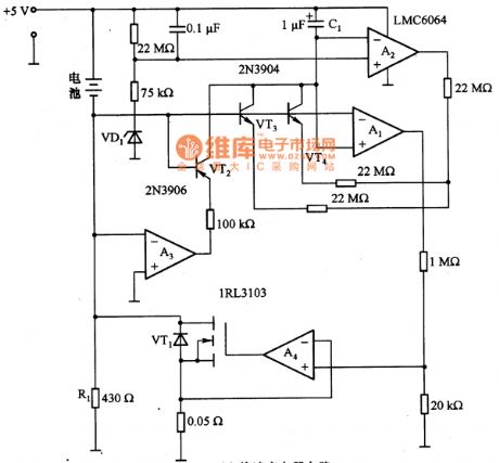
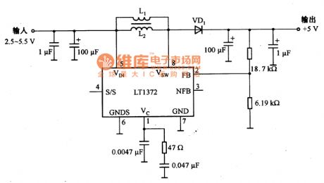
As what is shown in the picture, a and b are mini-UPS-circuits which are made up of quick charger circuit and main circuit. Picture 2(a) is quick charger circuit which use the way of quick charge to extend the life of the battery. The circuit made up of the operational amplifiers of A1 to A4 and related components manages the three working mode of the battery, which are charging, discharging and recharging. During charging the battery, it needs about 0.5A current and two to three hours. (View)
View full Circuit Diagram | Comments | Reading(2449)
A digital clock standard 60HZ time-based circuit
Published:2011/6/8 7:10:00 Author:Fiona | Keyword: A digital clock standard 60HZ time-based
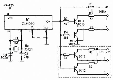
CD4060 is a 14-bit binary serial counter / oscillator frequency divider. Oscillator and External crystal R1, C1, C2 constitute the 30720Hz oscillator circuit; another part is the 14 frequency divider. Use the former 9 levels divider, and its frequency is 512.The standard 60Hz signal obtained by the oscillator output through the frequency division output from the Q9, as the standard base signal of the digital clock circuit. BG1, BG2 constitute a 60Hz signal synchro switch, Under the effect of 60Hz signal, BG1, BG2 conduct alternately, BG1 collector and BG2 emitter respectively connected todouble-negative-type display 1 and and 2 feets, ensure that the double-negative-type display works properly.
(View)
View full Circuit Diagram | Comments | Reading(3047)
TV remote controller 03
Published:2011/6/9 3:06:00 Author:TaoXi | Keyword: TV, remote controller
TV remote controller 03
(View)
View full Circuit Diagram | Comments | Reading(752)
The circuit diagram only permitting small DC singal voltage
Published:2011/5/20 19:56:00 Author:leo | Keyword: circuit diagram, small DC singal voltage
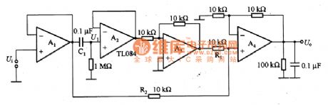
As what is shown in the picture, this is a circuit that only permits the small DC electronic current to pass through. If the inputting signal Ui is a sinusoidal waveform with the asymmetric peak value, and if the VFM is 11V and negative peak is -9 V, this waveform has small DC voltage. In some application, it needs to output the small DC signals and eliminate the AC signals which common low-pass filter cannot do but this circuit can make it come true. In this circuit, the buffer A1 buffers the inputting signals, and then the voltage of the buffered signals comes through the capacitor C1 and is coupled to a complete AC waveform voltage U1. (View)
View full Circuit Diagram | Comments | Reading(751)
| Pages:1764/2234 At 2017611762176317641765176617671768176917701771177217731774177517761777177817791780Under 20 |
Circuit Categories
power supply circuit
Amplifier Circuit
Basic Circuit
LED and Light Circuit
Sensor Circuit
Signal Processing
Electrical Equipment Circuit
Control Circuit
Remote Control Circuit
A/D-D/A Converter Circuit
Audio Circuit
Measuring and Test Circuit
Communication Circuit
Computer-Related Circuit
555 Circuit
Automotive Circuit
Repairing Circuit