
Circuit Diagram
Index 1762
Multiple Voltage Rectifier Circuit
Published:2011/6/4 3:20:00 Author:Michel | Keyword: Multiple Voltage, Rectifier Circuit
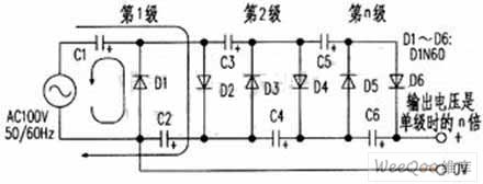
The Cochcroft&Walton circuit showed as the picture is a typical multiple voltage rectifier circuit.The half-wave voltage doubler comopsed of several diodes and capacitor connects in series and AC voltage charges and discharges capacitors C1~Cn in a half cycle in series-parallel way when it goes through diodes D1~Dn.Low ac input voltage can get several times of single half-wave voltage doubler's DC output voltage.Its work's principle:The mains supply charges C1 via D1 when it's negative half cycle. (View)
View full Circuit Diagram | Comments | Reading(863)
Additional Circuit of Simple Anti-theft and Alarm Telephone
Published:2011/6/4 9:27:00 Author:Michel | Keyword: Anti-theft and Alarm Telephone, Additional Circuit
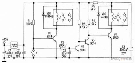
The author designs an additional circuit for anti-theft and alarm modified by finished telephone afer analyzing.Its material and facture are easy,cost is low,operation is convenient and it's safe and reliable.
Introduction to principleThe circuit is as the picture.K is reed pipe and V1 conducts,the fork reed switches's absorption of drive relays J1 is equal to that the telephone is off-hook . Another control signal amplifies via V2、V3 when it goes through R3 and C3's delay(RC in the picture is about 6s).V4 drive relay J2 is equal to redial key of the control telephone. (View)
View full Circuit Diagram | Comments | Reading(651)
Serial Adjustment Stabilized Voltage Supply Circuit
Published:2011/6/4 22:28:00 Author:Michel | Keyword: Serial Adjustment, Stabilized Voltage, Supply Circuit

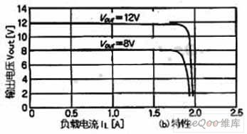
The right picture is adjustable stabilized voltage power which uses crystal triode to output voltage.This circuit adjusts the output voltage by changing high-power crystal triode, tr1's voltage of load series. The output voltage,Vout,depends on A'svoltage,namely,Vref+VBE2.In the right formula,Vref(5.1V)is the voltage of voltage regulator diode,VBE2 is the emitter-to-base voltage of crystal triode Tr2,VR1 is variable resistor.Variable range of VR1 is 0~5kΩ so the variable range of output voltage is 7.6~12.8V.When VR1 sliding parts contact undesirable, the output voltage will be a minimum voltage. (View)
View full Circuit Diagram | Comments | Reading(623)
Simplified PWM DC Servo Circuit by Using NE5560
Published:2011/6/4 22:42:00 Author:Michel | Keyword: PWM DC Servo, Circuit
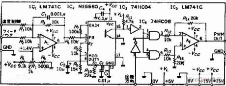
Circuit's Principle
When the linear drive DC servos the motor,the heating quantity will increase if the output transistor's power drops.On high-power conditions,usually,pulse amplitude drive mode are used like this circuit.The heating is controlled through incresing power by switching transistor's switch.The PWM circuit can be consistued by division elements.But this circuit uses part of ICNE5560 to simplify the circuit.OP amplifier A1 is error amplifier.
Speed control signal is proportional to deviation.The speed feedback terminal inputs rotate speed sensor signal.
(View)
View full Circuit Diagram | Comments | Reading(1944)
Simplified Synchronous Detection Circuit by Using Analog Switch and Differential Amplifier
Published:2011/6/4 22:46:00 Author:Michel | Keyword: Analog Switch, Differential Amplifier, Synchronous Detection Circuit
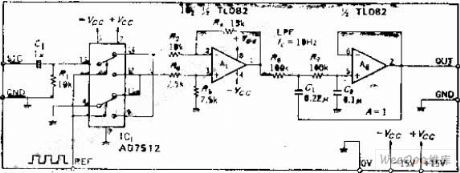
Circuit's FunctionThe full-wave rectifying type synchronous detection circuit also can be composed by alterindg differential amplifier's input signal.Its basic work principle is similar to the same frequency detection circuit of low-frequency drift polarity converting mode.It uses differential amplifier with informal parameters to receive the output of the two-way switch analog switches.The output DC stability of this circuit is high.It can be used in synchronous detection circuit which uses dozens of KHZ low frequency as low-frequency lock-in amplifier because it adopts analog switch. (View)
View full Circuit Diagram | Comments | Reading(1809)
The IC Whole Wave Synchronous Detection Circuit with Analog Switch
Published:2011/6/10 3:30:00 Author:Michel | Keyword: Analog Switch, IC, Whole Wave, Synchronous Detection Circuit

Circuit's Functions The total wave synchronous detection circuit which is widely used inthe low frequency range and its output pulse wave does not contain fundamental wave.Thus its requirements on low-pass filter cutoff performance can be relaxed.Half wave output circuit switch rectifier high frequency parts of Switch Circuit's Half Wave Synchronous Detection Circui can be showed as the formula:e1=1/π+1/2sinwt-2/3coswt+2/15cos4wt……In the formula,the first one was the DC component and the second is the base wave, the amplitude is 1/2. This circuit is total wave rectifier system and its formula is
e0=2/π-4/3sin2wt-4/15sin4wt……
The DC component is 2π and it's bigger than the former because there is no fundamental wave.Thus the filter filers the higher harmonic for over 2 times. (View)
View full Circuit Diagram | Comments | Reading(3022)
Half Wave Synchronous Detection Circuit of Switch Circuit
Published:2011/6/10 2:37:00 Author:Michel | Keyword: Switch Circuit, Half Wave, Synchronous Detection Circuit
Circuit's Functions
Synchronous detection circuit is used to detect the signal drowned by noises,it isthe most important circuit units of submerged phase-locked amplifier and it has many practical way.This circuit belongs to the synchronous detection's basic way,which uses a switch circuit to test phase difference.And its output voltage EO = EXCOS φ,that's to say,it can get signal amplitude and phase φ.If the reference signals is the same phasewith the unknown signal, it can obtain the average DC voltage output.For example,cutoff frequency of lower level low-pass filter is dropped, noises' constant efficiency width will be narrowed and S/N ratio will be improved. (View)
View full Circuit Diagram | Comments | Reading(473)
Simple PWM Circuit of Direct Modulation Self Excited Oscillation Circuit
Published:2011/6/9 22:24:00 Author:Michel | Keyword: Direct Modulation, Self Excited, Oscillation Circuit, Simple PWM Circuit
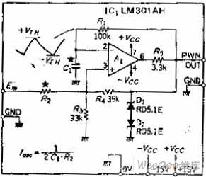
Circuit's FunctionsThe astable multivibrator which uses OP amplifier can get the oscillation ouput which has symmetrical postive and negative 1:1 dutyfactor.The pulsewidth can be modulated if the threshold voltage is altered from the outside and this circuit is very simple.Using CR charing and discarging circuit has a bad influence on the large modulation input linear.The oscillation frequency stability depends on the time, so often CR stability is not high. However,it can be used as a PWM power to control circuit.
Circuit's Work PrincipleIn this circuit,, oscillation frequency voltage depends on lagging voltage +VE and -VE's cycles if there is no input resistance R2. (View)
View full Circuit Diagram | Comments | Reading(1523)
Transistor Actinometer Circuit
Published:2011/6/3 12:30:00 Author:Michel | Keyword: Transistor, Actinometer Circuit
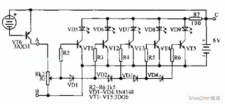
When solar cells are exposed to light,the generating voltge gets VT6 on state.VT6's conduction is proportional to the degree of light intensity.VT6 conducting electricity drops in R1,VT1 ~ VT5 base gets positive voltage.Thus VT1 ~ VT5 are in different working condition and some of VD5~VD9 are bright and some are dark.The intensity of the signal level isindicated,which means the intensity of illumination is also indicated. (View)
View full Circuit Diagram | Comments | Reading(862)
Optical Coupling Phone Anti-theft Device Circuit
Published:2011/6/3 12:09:00 Author:Michel | Keyword: Optical Coupling, Phone Anti-theft Device Circuit
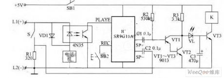
This transponder will tell your place or contact number to your friend when you friend calls you and you are outside.This transponder is safe and reliable and it will not be disturbed by busy signal.
Work's Principle
The optical coupling phone answer circuit is showed as the pictureThe SRG10A is 10S audio record circuit.Please press SB2 to switch on the power.What you want to tell your friend will be recorded via carried in electret microphone(this is not be drawn in the picture) Please press SB1 when you go out.When it's static state, the clad pipe's collector voltage composed of VT1 and VT2 is around 0.65V and both VL and VT3 are off. (View)
View full Circuit Diagram | Comments | Reading(680)
-90° Phase-shifting Circuit (Variable in 0~-180°)
Published:2011/6/4 22:14:00 Author:Michel | Keyword: -90° Phase-shifting Circuit, Variable in 0~-180°
The ±90°phase-shifting circuit with flat frequency characteristics can shift circuit in 0~+180°.Circuit's Work PrincipleThe work's principle is same with the ±90°phase-shifting circuit with flat frequency characteristics and it only changes the polarity of the phase.Here only the calculation method of the phase variable range is instructed.When FO is equal to 1KHZ,φis equal to -60~-120° and ,CO is equal to 0.01UF,RO is equal to 15.92K.If the RO is variable,phase angle,φ=-2TAN(RX/R0)and when RX is equal to RO,φis 90°. (View)
View full Circuit Diagram | Comments | Reading(399)
High-speed Absolute Value Circuit of OP Amp with Phase Delay Compensation
Published:2011/6/4 0:16:00 Author:Michel | Keyword: OP Amp, Phase Delay Compensation, High-speed Absolute Value
Circuit's Functions
If the signal frequencyis more than hundreds of KHZ,the output waveform will be disorder or itssensitivity will drop when we use absolute value of general OP amp. (View)
View full Circuit Diagram | Comments | Reading(2908)
NE602 Direct Variable Frequency Circuit
Published:2011/6/4 23:19:00 Author:Michel | Keyword: Direct Variable Frequency, Receiver Circuit
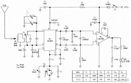
Push-pull output of NE-602(That's to say,tube feet 5 and feet 4 are used together)is more advanced than one-port output.Dillon points out that balanced output improves performance,especially its suppressionof AMBOB.At the same time,0.47μF capacitor is helpful to AM's breakthrough which connects across NE-602 output port. (View)
View full Circuit Diagram | Comments | Reading(8699)
MICRF007 Wireless Receiving Circuit
Published:2011/6/5 0:06:00 Author:Michel | Keyword: Wireless Receiving Circuit
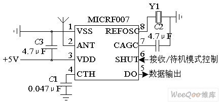
The wireless receving circuit is showed as above and MICRF007 is its core.MICRF007 is Micrel company launched monolithic UHF ASK/OOK(conduction - shutoff key )superheterodyne wirless receiver chips.MICRF007 adopts SOP (M) - 8 encapsulation.The chip inside circuit divided into UHF's convertor,OKK demodulator and reference control.UHF's convertor contains RF amplifier,mixer,intermediate frequency amplifier,bandpass filter,peak detectors,synthesizer and AGC control circuit.OKK demodulator contains low-pass filter, comparators.Benchmark oscillator and control logic circuit are included in reference control circuit. (View)
View full Circuit Diagram | Comments | Reading(1079)
Amplifier Circuit of FM Transmitter Main Frequency Power
Published:2011/6/5 0:42:00 Author:Michel | Keyword: FM Transmitter, Main Frequency Power, Amplifier Circuit
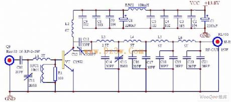
This power amplifier can extend 1-2W、88-108MHZ FM transmitter power to 10-15W.It uses single pipe c class amplifier and low-pass filter.It has higher conversion efficiency andstrong suppersion of considered wave.
Principle Figure
The circuit is showed as above.It adopts high-power transmitting tube C1972 and parameters are as follows:175MHZ,4A,25W,power gain ≥8.5db.As the pictures'parameters,the work center frequency is about 98MHZ.When the input radio-frequency power is about 2W,the rating output can reach 15W.The center frequency of former stage adjusts part of components to make sure that any frequency port among 88~108MHZ can reach rating value when it outputs. (View)
View full Circuit Diagram | Comments | Reading(3714)
Temperature Compensation Generating Circuit of ±10MV / ℃ Compensating Voltage
Published:2011/6/5 2:09:00 Author:Michel | Keyword: Compensating Voltage, Temperature Compensation
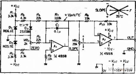
Circuit's FunctionsWhen DC amplifier disorder drift is linear and the disorder drift can be offsetted if this circuit's output is compensated to the circuit.This circuit is different from simple diode compensation circuit,it can freely set benchmark temperature and compensation slope.Thus the whole circuit can be regulated.
Circuit's Work Principle
Like using ordinary silicon diodes ,temperature sensor can obtain about -2.2MV/℃ variation.OP amplifier A1 moves the positive under reference temperature to zero and it can get +10MV/℃ output when the amplifier amplifies parts to 5 times.
(View)
View full Circuit Diagram | Comments | Reading(548)
6V to 14V Booster Power Circuit of Discrete Device
Published:2011/6/6 23:38:00 Author:Michel | Keyword: Discrete Device, 6V to 14V, Booster Power Circuit
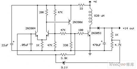
One schmitt trigger oscillator is used to drive the transistor and inductance energies stores in the inductance.The output voltage depends on load voltage and oltage regulator diode.This circuit's efficiency is about 80 %, and it also adopts the inductance with high Q value. (View)
View full Circuit Diagram | Comments | Reading(904)
Load Power Adjustor Five
Published:2011/5/22 0:45:00 Author:Michel | Keyword: Load Power Adjustor, Five

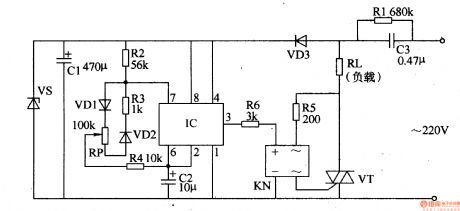
The bearing power adjustor introduced in the example is made from 555 time-base intergrated circuit with the features of simple circuit and manufacture.It can be used to adjust fun's speed,jacklight's light and electric heating appliance's temperature.
Circuit's Work PrincipleThe bearing power adjustor circuit is composed of power supply circuit,ultra-low frequency oscillator and control operation circuit and it is showed as the picture of 5-58.The power supply circuit consists of reduction voltage capacitor,C3,drain resistor,R1,commutation diode,VD3,filter capacitor and Zener diode,VS. (View)
View full Circuit Diagram | Comments | Reading(514)
Load Power Adjustor Six
Published:2011/5/22 0:48:00 Author:Michel | Keyword: Load Power Adjustor, Six
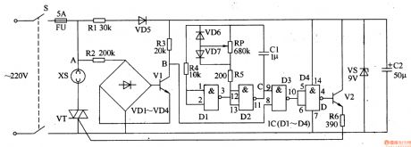
Theload power adjustor introduced in the example has the features of low power dissipation(self-power dissipation is only 1w)and broad regulating range(It can be adjusted from no output to all output).This adjustor can adjust electric heating appliance and fun's power.
Circuit's Work Principle The bearing power adjustor circuit consists of power supply circuit,zero cross impulse detection circuit,multivibrator type oscillator,control operation circuit and it is showed as the picture 5-59.The power supply circuit is composed of power switch,S,fuse,FV,current-limiting resistor,R1,commutation diode,VD5,filter capacitor,C2 and voltage regulator diode,VS. (View)
View full Circuit Diagram | Comments | Reading(445)
Adjustable AC Power Supply Nine
Published:2011/5/20 2:50:00 Author:Michel | Keyword: Adjustable AC , Power Supply, Nine
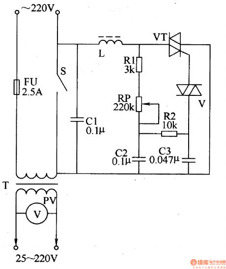
Alternating current power supply of different voltage grade is often used when we maintain household appliances.The alternating current power supply introudced in the example with the function of isolation can be used as maintenance power supply of household appliances such as color TV and its output voltage is 25-220V.
Circuit's Work Principle
This alternating current power supply circuit is composed of voltage regulation circuit and isolation output circuit and it is showed as the picture 5-62.The voltage regulation circuit consists of inductor,thyristor,VT,bidirectional trigger diode,V,resistor,R1 and R2,potentiometer,RP and capacitor C1-C3.
(View)
View full Circuit Diagram | Comments | Reading(2576)
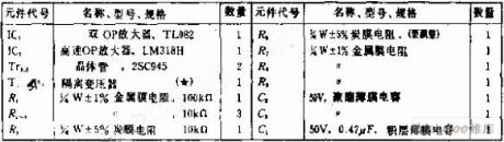
| Pages:1762/2234 At 2017611762176317641765176617671768176917701771177217731774177517761777177817791780Under 20 |
Circuit Categories
power supply circuit
Amplifier Circuit
Basic Circuit
LED and Light Circuit
Sensor Circuit
Signal Processing
Electrical Equipment Circuit
Control Circuit
Remote Control Circuit
A/D-D/A Converter Circuit
Audio Circuit
Measuring and Test Circuit
Communication Circuit
Computer-Related Circuit
555 Circuit
Automotive Circuit
Repairing Circuit