
Circuit Diagram
Index 1778
Typical Application Circuit of UC3842 Overvoltage and Overcurrent Protection
Published:2011/6/7 0:08:00 Author:Michel | Keyword: Overvoltage and Overcurrent Protection, Typical Application Circuit
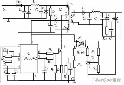
The typical application circuit of UC3842 overvoltage and overcurrent protection picture is showed as above.
Overcurrent Protection Principle
When load current exceeds rating value or the output shorts,which causes that current is added to switch tube V4 ,R7's voltage feedbacks to feet.When R7's voltage exceeds 1V and the conduction width narrows down cuased by inside current amplifier and the output voltage drops,meanwhile it makes the UC3842 work's voltage drop.When it is lower thansetting voltage,over-current protection circuit starts to work to protect power tube.Power supply resumes work when short circuit phenomenon vanishes.
(View)
View full Circuit Diagram | Comments | Reading(10631)
555 simple motor phase failure and overcurrent protection device circuit
Published:2011/6/10 21:45:00 Author:nelly | Keyword: motor phase failure, overcurrent protection device

As shown in the figure 10-21, AC hypotension rectifier circuit provides this circuit with VDD=12V voltage power. The current transformer takes anyone from the three phase motor, after its AC signal is rectificated and filtered, it is used as the monostable delay circuit's comparative voltage which is composed of 555. When it is connected to power supply, 555's 2 foot is low level, 555 is set, 3 foot is high level, J has no action. The short steady time td=1.1(R1+R2)C2, the time constant can be changed by adjusting RC2. When the motor works normally, adjusting RP1, the motor current is turned to lower than 2/3 VDD voltage by LH, it is added to IC's 6 foot.
(View)
View full Circuit Diagram | Comments | Reading(2287)
555 simple electric leakage protector circuit
Published:2011/6/10 22:02:00 Author:nelly | Keyword: electric leakage, protector

As shown in the figure 10-7, the protector is composed of transformer, preamplifier stage and monostable delay circuit and relay. The protection action current is lower than 3mA, the action time is lower than 0.1s.
The transformer HL adopts high conductive magnetic ring, primary fire line and zero line parallel winding 5 turns, secondary polarity winding 500 turns. In normal times, HL's primary line current is in balanced state, secondary polarity does not output signal. When it comes load electric leakage, secondary polarity has signal current, after amplified by VT1, 555's 2 foot is lower than 1/3 VDD, 555 is set, J1 pulls in, J1-2, J1-3 cut off, they are electric leakage protection. VT1 adopts MOSFET, it is voltage control tube, the static work current Ip is about 0.9mA.
(View)
View full Circuit Diagram | Comments | Reading(1202)
555 serial switch regulated power supply circuit
Published:2011/6/10 22:18:00 Author:nelly | Keyword: switch, regulated power supply
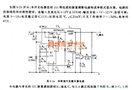
Compared to the usual 555 pulse width modulator, this circuit connects resistance R3 between C1 and 2, 6 feet, it can decrease C1's voltage amplitude. The output voltage sample and amplification circuit are composed of VT2, R5, R6, R7, RP1, RP2, the feedback voltage can be changed by adjusting RP1 and RP2, then the duty ratio of switch square wave and output DC voltage also can be changed. VT1 adopts P groove VMOS tube MTM10P5, the rated current is about 10A. The energy storage induction is about 1mH. D is Fly-wheel diode.
(View)
View full Circuit Diagram | Comments | Reading(1345)
555 hig voltage delay time contact controlled circuit
Published:2011/6/7 1:53:00 Author:nelly | Keyword: high voltage, delay time, contact cotrolled

This circuit is always used in the occasion that the filament need preheat in the vacuum tube equipment. It makes the filament has adequacy time to avoid the cathode added the high pressure under the cold state. As shown on the figure 9-48, the 555 is in the reset mode because the C1's voltage can't mutant. The 555 will reset with the C1 charged when the 2 foot's potential is lower than 1/3VDD. The 3 foot will be the high power level and the J will be pull-in. The contact will contact the high voltage. The delay time, td=1.1RP1C1. The max delay time is about 4 minutes and can use the RP1 to change.
(View)
View full Circuit Diagram | Comments | Reading(960)
Ward Caller Seven
Published:2011/6/3 21:49:00 Author:Felicity | Keyword: Ward Caller,
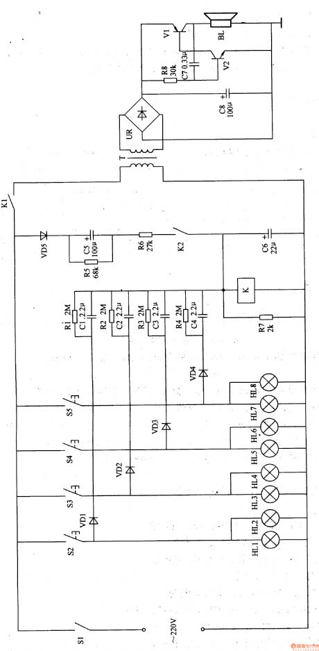
When S1 is switched on, the whole appliance is under standby state. And when one of the call buttons 52-55 is pressed, the indicator in the branch is on, and the capacitor is charging, then K turns on and closes, the normally open contact of K switched on, and C5 is charging to keep K closes. The audio oscillator consists of V1, V2, R8 and C7 works to drive BL to send out calling sound. As the charging current of C5 decreases, the voltage of C5 drops too. When the voltage of C6 drops to a certain value, K releases and the audio circuit stops working.
(View)
View full Circuit Diagram | Comments | Reading(580)
Mine spray dedusting controller circuit diagram
Published:2011/6/10 6:26:00 Author:Lucas | Keyword: Mine spray, dedusting, controller
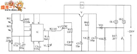
The mine spray dedusting controller circuit consists of +6 V power supply circuit, light control circuit, LED indication circuit and the solenoid valve control circuit, and the circuit is shown as the chart. +6 V power supply circuit consists of the illuminating lamps EL1, EL2, resistors R4, R5, switch S, diodes VD1, VD2, filter capacitors C5, C6, Zener diode V and transistor VS. Light control circuit consists of the photosensitive resistors RGI, RG2, potentiometers RP1, RP2, capacitors C1 ~ C3 and the time-base integrated circuit IC. Solenoid valve control circuit is composed of the internal circuit of IC, resistors R2, R3, thyristor VT, capacitor C4 and electromagnetic valve YV. LED indicating circuit is composed of the resistor R1 and LED VL. R1 and R4 select 1/4W metal film resistors; R2 uses 1W film resistor.
(View)
View full Circuit Diagram | Comments | Reading(1160)
The LT current sensor wiring circuit
Published:2011/6/10 21:59:00 Author:qqtang | Keyword: current sensor, wiring circuit
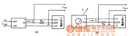
Figure:The LT current sensor wiring circuit (View)
View full Circuit Diagram | Comments | Reading(556)
Binary-Decimal Counter Circuit Diagram
Published:2011/6/9 3:56:00 Author:Vicky | Keyword: Binary-Decimal Counter, CD4066, CD4013, CD4017
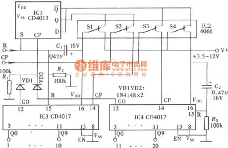
(View)
View full Circuit Diagram | Comments | Reading(1032)
Mine locomotive remote controller circuit diagarm
Published:2011/6/10 6:13:00 Author:Lucas | Keyword: Mine locomotive , remote controller
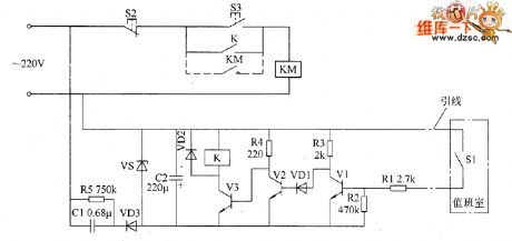
The mine locomotive remote controller circuit consists of transistors V1 ~ V3, capacitors C1 and C2, resistors R1 ~ R5, diodess VD1 and VD2, Zener diode VS and the control switch S1, and the circuit is shown as the chart. Stop button S2, start button S3, AC contactor KM and the normally open contact of K form the main control circuit of Stepless rope motor M (it is not shown in the circuit). VS, C1, C2, R5, and VD3 form the regulated power supply circuit, and the control switch S1 is installed in the duty room, then the one end is connected to the ground, and the other end is connected to R1 by wire. AC 220V voltage bucked by C1, rectified by VD3, filtered by C2 and stabilized by vs to provide 9V DC voltage for relay control circuit. R1 ~ R5 use 1/4W carbon film resistors or metal film resistors.
(View)
View full Circuit Diagram | Comments | Reading(722)
555 sectional timing circuit
Published:2011/6/7 1:12:00 Author:nelly | Keyword: sectional, timing
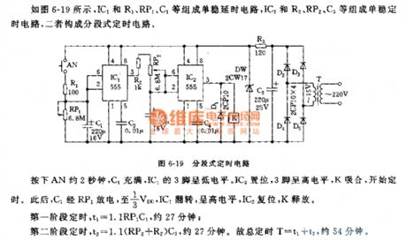
As shown on the figure 6-19, the mono-stable time delay circuit consits of the IC1 and R1,RP1,C1. The mono-stable timing circuit consists of the IC2 and R2,RP2,C3.They constract the sectional timing circuit. Pressing the AN about 2s, the IC1's 3 foot is low power level. The IC2 reset, the 3 foot is high power level and the K will be pull-in. Then the C2 will discharge by the RP1 to the 1/3VDD. The IC1 will flip and be the high power level. The IC2 will reset and K will release. The first timing, t1=1.1RP1C1, about 27 minutes. The second timing, t2=1.1(RP2+R2)C3, about 27 minutes. The total timing, T=t1+t2, about 54 minutes. (View)
View full Circuit Diagram | Comments | Reading(744)
555 novel long timer circuit
Published:2011/6/7 0:56:00 Author:nelly | Keyword: novel, long timer
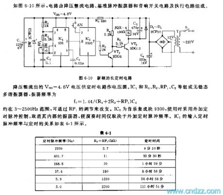
As shown on the figure 6-10, the circuit consists of the hypotension rectifying circuit,reference pulse oscillator, audio switch circuit and executive circuit. The timer circuit's voltage source is 4.8V. The actable multivibrator consists of the IC1 and R1,R2,RP1,C2. The oscillation frequency: f0=1.44/(R1+2R2+RP1)C2. It can be regulated by the RP1. The IC2 is the 9300 music manifold block. It can be controlled by the pulse. Its performance time only depends on the pulse frequency in addition after cancelling its oscillator. The ralations between the IC2's input time pulse frequency and the time are shown on the figure 6-1. (View)
View full Circuit Diagram | Comments | Reading(1090)
High voltage static generator circuit diagram 2
Published:2011/6/9 3:52:00 Author:Lucas | Keyword: High voltage , static generator
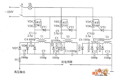
The high voltage static generator circuit is composed of the oscillating boost circuit and voltage doubling rectifying circuit, and the circuit is shown as the chart. Oscillation step-up circuit is composed of the resistors R1 ~ R3, capacitors C1 ~ C3, thyristors VT1 ~ VT3, diodes VD1 ~ VD6 and step-up transformers T1 ~ T3. Voltage doubling rectifying circuit is composed of the diodes VD7 ~ VD16 and capacitors C4 ~ C13. R1 ~ R3 select 1/2W metal film resistors. C1 ~ C3 select CBB capacitor with the voltage in 630V; C4 ~ C13 select high voltage ceramic capacitors with the voltage in 1kv. VD1 ~ VD6 use 1N4007 silicon rectifier diodes; VD7 ~ VD16 use high voltage silicon rectifier stack with the withstang voltage in 20kv.
(View)
View full Circuit Diagram | Comments | Reading(1550)
Static electricity eliminator circuit diagram 1
Published:2011/6/9 4:01:00 Author:Lucas | Keyword: static electricity eliminator
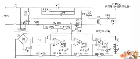
The static electricity eliminator circuit is composed of 12V regulated power supply circuit, pulse boosted circuit and LED output indication circuit, and the circuit is shown as the chart. 12V regulated power supply circuit is composed of the power transformer T1, bridge rectifier UR, filter capacitor C1 and the three-terminal voltage regulator integrated circuit IC1. Pulse booster circuit is composed of the resistors R1 ~ R5, capacitors C2 ~ C5, thyristor VT, potentiometer RP, diodes VD1 ~ VD3 and the step-up transformer T2. Output voltage indication circuit consists of resistors R6 ~ R13, light emitting diodes VL1 ~ VL4 and operational amplifier integrated circuit IC2 (N1 ~ N3). R1, R4 and R5 select 1/2W metal film resistors; R2 uses 3W metal film resistor; R3 uses 1W metal film resistor; R5 ~ R13 select 1/4W metal film resistors or carbon film resistors.
(View)
View full Circuit Diagram | Comments | Reading(2117)
555 Sequence timer control circuit
Published:2011/6/7 0:28:00 Author:nelly | Keyword: Sequence, timer control
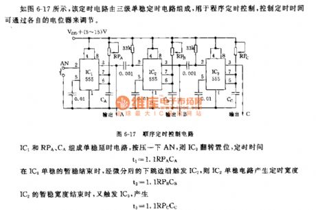
As show on the figure 6-17, this timer circuit consists of the three-level monostable timer circuit. It can be used in the program's timer control and its time can be regulated by thePotentiometer. The monostable delay circuit consists of the IC1 and RPA, CA. Press the AN, the IC1 will filp and reset. The time: t1=1.1RPACA. When the IC1's transient stability is over, the foot edage will trig the IC2, then the IC2 will produce the timer width: t2=1.1RPBCB. The IC2 will trig the IC3 when its transient stability width is over, t3=1.1RPCCC. (View)
View full Circuit Diagram | Comments | Reading(1575)
The sound and light alarm circuit diagram 1 for industrial instrumentation
Published:2011/6/9 4:40:00 Author:Lucas | Keyword: sound , light, alarm, industrial instrumentation
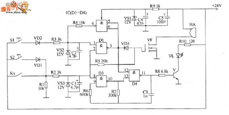
The sound and light alarm circuit for industrial instrumentation is composed of the detection control circuit, bistable trigger, LED flash circuit, sound alarm circuit and +12 V voltage regulator circuit, and the circuit is shown as the chart. Detection control circuit is composed of controlled contact of industrial instrument (controlled electric contact) Kx, resistors R1, R2, zener diode VS3 and capacitors C1. LED flash circuit consists of the D3, D4 which are inside of NAND gate integrated circuit IC (D1 ~ D4), resistors R6 ~ R8, R10, capacitor C3, transistor V and LED VL. Sound the alarm circuit is composed of resistor R5, field-effect transistor VF and alarm HA. R1 ~ R8 select l/4W metal film resistors.
(View)
View full Circuit Diagram | Comments | Reading(1261)
555 Monitoring output transformer circuit
Published:2011/6/4 6:45:00 Author:nelly | Keyword: Monitoring, output transformer
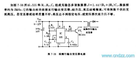
As shown on the figure 7-38, the actable multivibrator consists of the 555 and R1,R2,C1. f=1.44/(R1+2R2)C1, the oscillation frequency is about 2kHz. Its output connect the output transformer through the power amplifier. It gets kilovoltage DC voltage by being boosted and high voltage silicon's rectification. If the transformer or the silicon pile's quality is bad, the high voltage can't reach the identifiable voltage.
(View)
View full Circuit Diagram | Comments | Reading(771)
Memory Strengthener (the 2nd)
Published:2011/5/19 21:24:00 Author:Felicity | Keyword: Memory Strengthener (the 2nd)
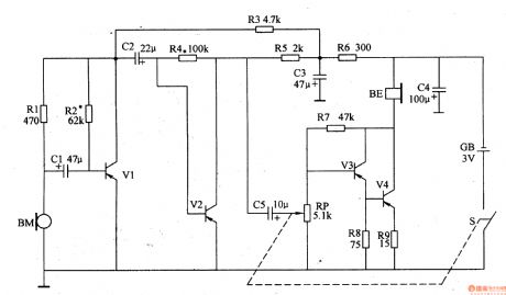
Work of the circuit
The circuit consists of mike BE, three-step amplifier circuit and earphone. (It is showed in picture 9-76.). BM turns the sound signal it collects into electric signal. The signal will be amplified. Then the amplified signal will drive BE to make sound which is louder.
If you change the value of RP you can change the volume. (View)
View full Circuit Diagram | Comments | Reading(549)
555 multiple signals generator circuit
Published:2011/6/10 2:27:00 Author:nelly | Keyword: multiple signals, generator
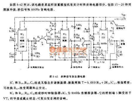
As shown on the figure 8-42, this circuit is the timing and audio circuit parts of the monitoring device model. It includes 15s~20s periodic pulse waveform, second signal and 800Hz audio circuit. The actable multivibrator consists of the IC1 and R16,R19,C12. The oscillation period: T=0.693(R18+2R19)C12. According to the need, we can use the R13 to change the period and the duty ratio. The clock oscillator consists of the IC2 and R23,R24,C13. The IC3 is a 800Hz audio oscillator, its control site's 5 foot is controlled by the VT1's turn-on or cut-off to output variation tone. (View)
View full Circuit Diagram | Comments | Reading(724)
The sound and light alarm circuit diagram 2 for industrial instrumentation
Published:2011/6/9 4:33:00 Author:Lucas | Keyword: sound , light alarm, industrial instrumentation
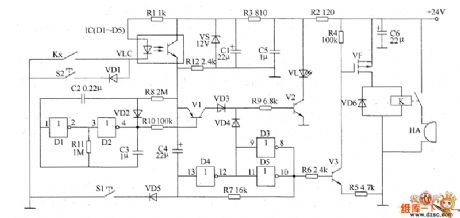
The sound and light alarm circuit for industrial instrumentation is composed of the +12 V voltage-stabilizing circuit, switch control circuit, oscillator, bistable flip-flop, sound and light alarm circuit, and the circuit is shown as the chart. +12 V voltage-stabilizing circuit consists of resistors R2, R3, filter capacitors C1, C5, C6 and regulator diode VS. Switch control circuit consists of resistors R1, R12, optocoupler VLC and industrial instrumentation control contact (controlled electrical contact) Kx. Oscillator is composed of the D1, D2 which are inside of NOT gate IC IC (D1 ~ D5) and diode VD2, resistor R11, capacitors C2, C3. Bistable flip-flop is composed of the D3 ~ D5 which are inside of IC and resistor R7.
(View)
View full Circuit Diagram | Comments | Reading(1046)
| Pages:1778/2234 At 2017611762176317641765176617671768176917701771177217731774177517761777177817791780Under 20 |
Circuit Categories
power supply circuit
Amplifier Circuit
Basic Circuit
LED and Light Circuit
Sensor Circuit
Signal Processing
Electrical Equipment Circuit
Control Circuit
Remote Control Circuit
A/D-D/A Converter Circuit
Audio Circuit
Measuring and Test Circuit
Communication Circuit
Computer-Related Circuit
555 Circuit
Automotive Circuit
Repairing Circuit