
Circuit Diagram
Index 1779
Electronic Points Probing Instrument (the 1st)
Published:2011/6/6 10:08:00 Author:Felicity | Keyword: Electronic Points Probing Instrument (the 1st)
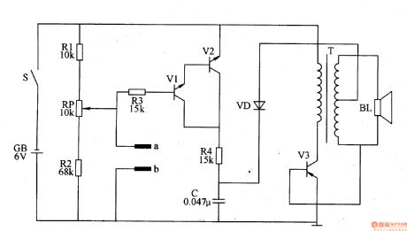
Work of the circuit
The circuit consists of probing poles, transistor V1-V3, resistor R1-R4, potentiometer RP, capacitor C, amplifier BL, diode VD, switch GB and battery GB. (It is showed in picture 9-38.)
Turn on power switch S. let the tester put the poles in their hands. Use the poles to test the relevant parts and body. When the acupoint is not tested, BL makes no sounds. When the acupoint is tested BL screams.
Change the value of RP to change the sensitivity of the circuit.
(View)
View full Circuit Diagram | Comments | Reading(547)
555 pressure sensing digital circuit
Published:2011/6/10 2:00:00 Author:nelly | Keyword: pressure, sensing, digital
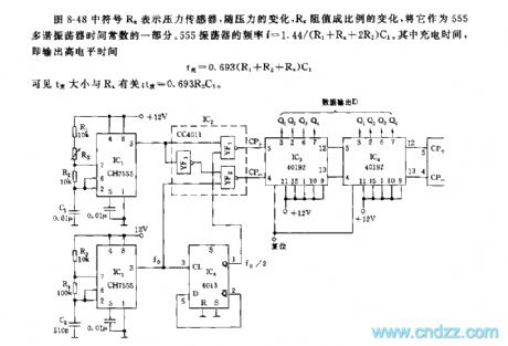
The RX on the figure 8-48 represents the pressure sensor. The Rx changes in proportion with the voltage's change. Taking it as the part of the multivibrator's time constant. The 555 oscillator's frequency: f=1.44/(R1+RX+2R2)C1. Its charge time which means outputing high power level time: t=0.693(R1+R2+RX)C1. we can find the t's big/small is relation to the Rx. (View)
View full Circuit Diagram | Comments | Reading(828)
Wireless remote electronic detonating device circuit diagram 2
Published:2011/6/9 6:17:00 Author:Lucas | Keyword: Wireless remote , electronic , detonating device
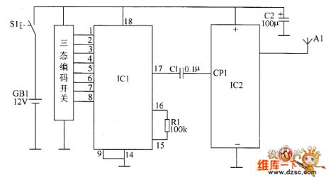
The wireless remote electronic detonating device is composed of the wireless remote transmitter circuit and wireless receiver initiator circuit. The wireless remote transmitter circuit is composed of control button S1, battery OBI, wireless encoding integrated circuit IC1, wireless transmitter integrated circuit IC2, resistor R1, capacitors U1, C2, transmitter antenna A1, and the circuit is shown as the chart. R1 ~ R4 select 1/4W metal film resistors; R5 and R6 select 1W metal film resistors. C1 and C3 select monolithic capacitors; C2 uses aluminium electrolytic capacitor with the voltage in 16V; C4 and C5 select electrolytic capacitor with the voltage in 630V. V1 chooses 58050 silicon NPN transistor; V2 uses BU406 high back pressure NPN silicon transistor.
(View)
View full Circuit Diagram | Comments | Reading(1462)
Electronic Massager (the 2nd)
Published:2011/6/6 8:18:00 Author:Felicity | Keyword: Electronic Massager (the 2nd)
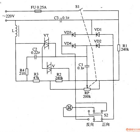
Work of the circuit
The circuit consists of AC pressure regulating circuit and rectification circuit. (It is showed in picture 9-35.)
Turn on switch S1. 220V AC separates into 2 parts. One charges C1 after being adjusted. And the other one changes into DC voltage and works as M’s working power. When the voltage of C1 reaches a constant value M starts working. (View)
View full Circuit Diagram | Comments | Reading(701)
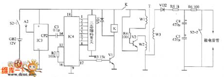
Wireless remote electronic detonating device circuit diagram 1
Published:2011/6/9 6:08:00 Author:Lucas | Keyword: Wireless remote , electronic , detonating device
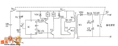
Wireless receiver initiator circuit is composed of the power circuit, wireless receiver control circuit, oscillation step-up circuit and charge-discharge circuit, and the circuit is shown as the chart. The power circuit consists of the battery GB, switch S (Sa, Sb), power indicator LED VL and current limiting resistor R6. Wireless receiver control circuit is composed of the wireless receiver module IC, resistors R1 and R2, transistors V1 and V2, relays K1 and K2 and diodes VD1, VD2. Oscillating boost circuit is composed of the normally open contact of K1, resistor R3, transistor V3, step-up transformer T and rectifier diode VD3. Charge-discharge circuit consists of resistors M and R5, capacitors C1 and C2, power switch Sb and the normally open contact of K2. R1 ~ R4 and R6 select 1/4W metal film resistors.
(View)
View full Circuit Diagram | Comments | Reading(915)
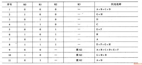
Scintillation Caution Light (4)
Published:2011/6/3 5:35:00 Author:Sue | Keyword: Scintillation, Caution, Light
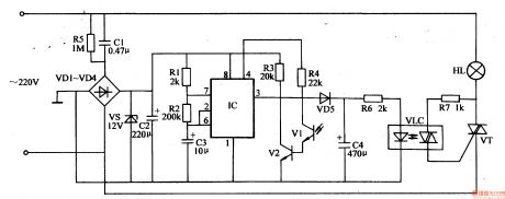
When the oscillator begins to work, IC's 3 pin outputs 1 Hz low frequency square form wave signals. When the signal is positive, VD5 is connected and VLC's LED is illuminated. VT is connected and HL is illuminated.
When the signal is negative, VD5 is disconnected. VLC's LED has a weaker light and HL's light becomes weaker.
Before HL goes out, another positive signal comes and it is illuminated again.
In the daytime, V2 is connected and IC's 4 pin has a low level. VLC and VT are disconnected. HL is not illuminated.
At night, VI has a high resistance value and IC begins to work. (View)
View full Circuit Diagram | Comments | Reading(603)
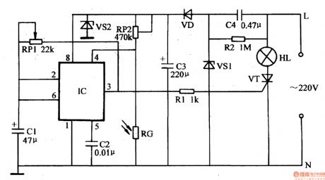
Scintillation Caution Light (3)
Published:2011/6/3 5:30:00 Author:Sue | Keyword: Scintillation, Caution, Light
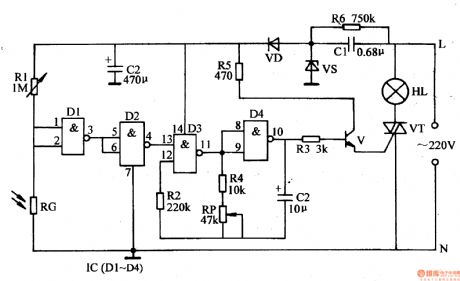
In the daytime, RG has a low resistance value. IC's 1 pin and 2 pin have low level and 3 pin has high level. The low frequency oscillator doesn't work. IC's 10 pin outputs oscillator signals and V is disconnected. VT is disconnected and HL is not illuminated.
When there is no light, RG has a high resistance value. IC's 1 pin and 2 pin have high level. 3 pin has low level and 4 pin has high level. The oscillator begins to work. IC's 10 pin outputs low frequency oscillator signals. V and VT are connected and HL is illuminated. (View)
View full Circuit Diagram | Comments | Reading(608)
Scintillation Caution Light (2)
Published:2011/6/3 5:24:00 Author:Sue | Keyword: Scintillation, Caution, Light
In the daytime, resistance RG has a low resistance value because of the light. IC's 4 pin has a voltage lower than 0.4V. The multivibrator doesn't work. 3 pin outputs low level, and VT is disconnected. HL is not illuminated.
When there is no light, RG has a high resistance value. IC's 4 pin has a voltage higher than 0.4V. The multivibrator begins to work. IC's 3 pin outputs high level and low level with a certain frequency. VT is connected from time to time. HL begins to twinkle. (View)
View full Circuit Diagram | Comments | Reading(506)
Light-Operated Night Lamp (3)
Published:2011/5/27 6:39:00 Author:Sue | Keyword: Light-Operated, Night Lamp
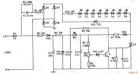
The 220V voltage will provide LED circuit with working voltage after reduction, rectification. Another circuit will provide light-operated electronic switch circuit with 15V ac voltage after reduction, rectification, filtration and stablization.
In the daytime, RG's resistance value is small because of the light. VS2 is connected and V is connected. VT is disconnected and VL1-VL8 are not illuminated.
At night, RG's resistance value becomes large. C5's voltage becomes lower. VS2 and V are disconnected. R8,R9 will provide VT with voltage. VT is connected and VL1-VL8 are illuminated. (View)
View full Circuit Diagram | Comments | Reading(1769)
Light-Operated Night Lamp (2)
Published:2011/5/27 6:34:00 Author:Sue | Keyword: Light-Operated, Night Lamp
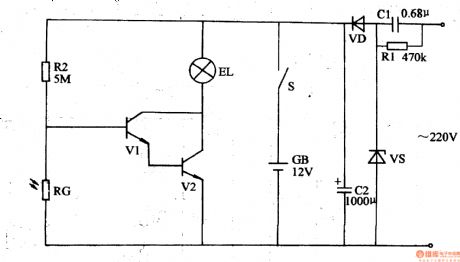
The power circuit consists of C1,R1,VS,VD,C2,S and GB.
The light-operated circuit consists of R2,RG,V1 and V2.
The alternating current voltage of 220V can provide EL and the circuit with 12V voltage after reduction, stablization, rectification and filtration. It can also charge GB by S.
In the daytime, RG will have a small resistance value because of the light, and V1,V2 are disconnected. EL is not illuminated. At night, RG has a large resistance value. Its voltage is higher than 1.4V and V1 V2 are connected. EL is illuminated. (View)
View full Circuit Diagram | Comments | Reading(587)
Light-Operated Night Lamp (1)
Published:2011/5/27 6:41:00 Author:Sue | Keyword: Light-Operated, Night Lamp
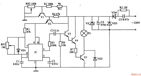
When the multivibrator begins to work, IC's 3 pin outputs pulse signals, which will illuminate EL after amplification.
When it is in the daytime or there is light, RG's resistance value will become small. V1 will be connected and V2 will be disconnected. IC stops working because of lack of power.EL is not illuminated.
When it is dark, RG's resistance value become larger. V1 is disconnected and V2 is connected. The multivibrator and the output circuit will begin to work and EL is illuminated. (View)
View full Circuit Diagram | Comments | Reading(615)
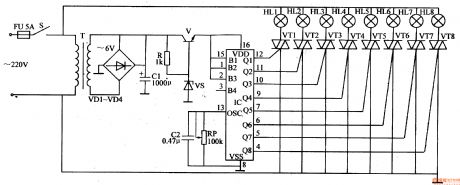
Illuminations Controller (1)
Published:2011/5/29 20:31:00 Author:Sue | Keyword: Illuminations, Controller
When S1 is connected, 220v voltage will generate +5V voltage after reduction, rectification,filtrition, which will be sent to IC,V0-V7. When IC begins to work, Y0-Y7 will output high level pulse, and V0-V7 will be connected. VT0-VT7 will be connected. 8 circuit illuminations will be turned on. When any transistor of V0-V7 is connected, its LED will be illuminated as monitor.
IC's OSCR terminal is connected with RP. When RP's resistance value is changed, the twinkle frequency of the illuminations will be changed. (View)
View full Circuit Diagram | Comments | Reading(456)
Illuminations Controller (2)
Published:2011/5/29 20:36:00 Author:Sue | Keyword: Illuminations, Controller
When S is connected, alternating current voltageof 220v will provide IC with 5v direct current voltage after reduction, rectification, filtrition and stablization.
When IC begins to work, its output terminal will output high level according to the set illuminating way. The transistors will control the illuminations.
The circuit connects IC's 1 pin 2 pin and 15 pin together, and makes the illuminating way vary from A to F automatically. (View)
View full Circuit Diagram | Comments | Reading(529)
Pulse Test Set (the 5th)
Published:2011/6/6 8:10:00 Author:Felicity | Keyword: Pulse Test Set (the 5th)
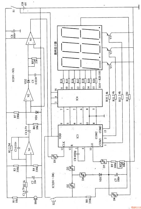
Work of the circuit
The circuit consists of power circuit, pulse signal testing and amplifying circuit, delaying resetting circuit and digital display circuit. (It is showed in picture 9-52.)
When you do the test, put BM on the position where the pulse is significant. Turn on power switch S1 and press the resetting control button. IC3 is ready to count.
BM turns the pulse signal into electronic signal. The signal then becomes the counting pulse. The pulse drives digital display to work after being adjusted. The number on the display changes with the pulse. The number displayed on the LED digital display is the jumping number of times of pulse per minute. (View)
View full Circuit Diagram | Comments | Reading(889)
Drunken Driving Limiter (the 2nd)
Published:2011/6/6 6:36:00 Author:Felicity | Keyword: Drunken Driving Limiter (the 2nd)
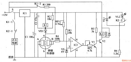
Work of the circuit
The circuit consists of the power voltage stabilizing circuit, LED instructing circuit, alcoholic sensitivity alcohol control circuit and control executing circuit. (It is showed in picture 7-161.)
Turn on the igniting switch S. The +12V voltage is adjusted by IC1 and C1 and provides working power to LED instructing circuit and alcoholic sensitivity alcohol control circuit.
If the driver is drunk and wants to turn on S. IC1 tests the sense of alcohol. The electric resistance will become smaller. The power circuit of igniting circuit is cut off. The driver cannot start the car. (View)
View full Circuit Diagram | Comments | Reading(579)
Pulse Test Set (the 4th)
Published:2011/6/6 8:09:00 Author:Felicity | Keyword: Pulse Test Set (the 4th)
Work of the circuit
The circuit consists of pulse signal testing and amplifying circuit and acousto-optic circuit. (It is showed in picture 9-51.)
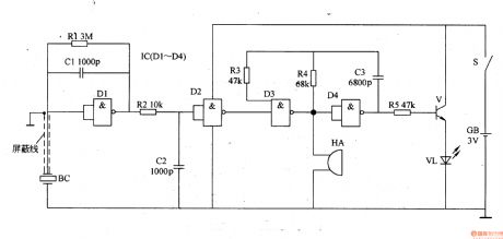
When you do the test, put BC on the position where the pulse is significant. Turn on power switch S. BC turns pulse signal into weak electronic signal. The electronic signal is amplified and reshaped. Then the signal makes the OSC work. HA makes the sound ‘tick, tick’ and VL shines. (View)
View full Circuit Diagram | Comments | Reading(542)
Pulse Test Set (the 2nd)
Published:2011/6/6 8:06:00 Author:Felicity | Keyword: Pulse Test Set (the 2nd)
Work of the circuit
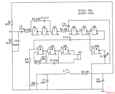
The circuit consists of power circuit, light sensor, reshaping amplifying circuit and acousto-optic circuit. (It is showed in picture 9-49.)
When we do not test the electric resistance is almost the same. HA does not make any sound and VL does not shine.
Put your figure on RG1 and the photopermeability change the electric resistance EG1. Voltage of point A changes slightly with the pulse. The signal is adjusted by amplifying circuit and makes acousto-optic circuit work. HA makes sound with the pulse. VL shines with the pulse. (View)
View full Circuit Diagram | Comments | Reading(531)
Pulse Test Set (the 1st)
Published:2011/6/6 8:05:00 Author:Felicity | Keyword: Pulse Test Set (the 1st)
Work of the circuit
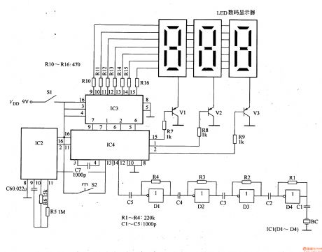
The circuit consists of signal amplifying circuit, OSC and counting indicating circuit. (It is showed in picture 9-48.)
When you use the pulse test set you should use a watch belt to press the sensor on the tester’s wrest (do press it tightly). Turn on the switch S the OSC starts working. The sensor BC turns the pulse jumping signal into electronic signal. The signal then will be amplified. It produces BCD code. BCD code is decoded and drives LED digital display to work. When the OSC works for 1min, the number displayed on the LED digital display is the jumping number of times of pulse. (View)
View full Circuit Diagram | Comments | Reading(760)
555 ultrasound remote control voice doorbell circuit
Published:2011/5/30 8:37:00 Author:TaoXi | Keyword: 555, ultrasound, remote control, voice doorbell
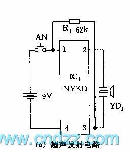
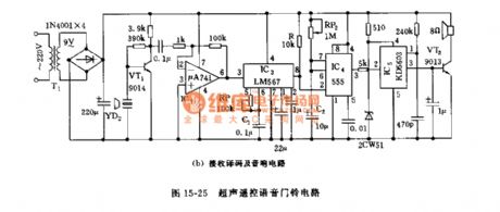
As the figure 15-25 shows, the doorbell is composed of the ultrasound launch circuit and the receiving decoding and audio circuit. This circuit can remote control the voice circuit at the distance of 10 meters.
The launcher uses the special ultrasound launch integrated circuit NYKD to drive the piezoelectric ceramic ultrasound emission sensor YD1 to send out the 40kHz ultrasonic wave. If you press AN, this circuit sends out a string of modulation ultrasonic pulse wave.
The IC3 uses the audio decoder LM567 which has the phase-locked loop (PLL). When there is no signal, the output port pin-8 has the high electrical level because of the R=10kΩ bias, when there is the input signal, it outputs the negative hopping pulse to trigger the IC4 monostable circuit. The center frequency f0 of the IC3 should be set at the 40kHz frequency emission.
(View)
View full Circuit Diagram | Comments | Reading(1117)
555 ultrasonic wave fish tank oxygen device circuit
Published:2011/5/30 9:23:00 Author:TaoXi | Keyword: 555, ultrasonic wave, fish tank, oxygen device
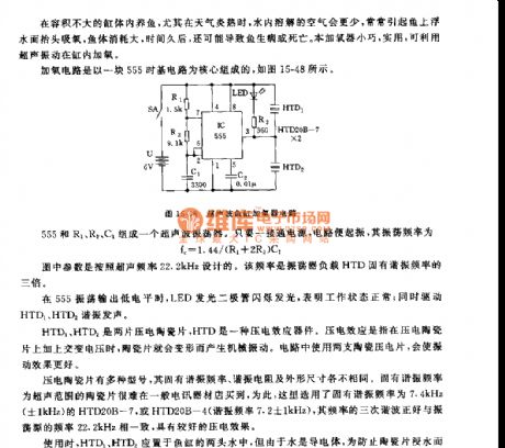
The oxygen device circuit uses the 555 time base circuit as the core, as the figure 15-48 shows.
The ultrasonic oscillator is composed of the 555 and R1,R2,C1. If you open the power supply, the circuit will start working, the oscillation frequency fc=1.44/(R1+2R2)C1.
The parameters are according to the design of ultrasonic frequency 22.2 kHz. This frequency is three times of the oscillator load HTD's inherent resonance frequency. When the 555 oscillation outputs the low electrical level, the LED has the flashing shine, this means the normal working condition; at the same time it drives the HTD1 and HTD2 to resonate.
The HTD1 and HTD2 are two piezoelectric ceramics, HTD is one kind of piezoelectric effect device.
(View)
View full Circuit Diagram | Comments | Reading(974)
| Pages:1779/2234 At 2017611762176317641765176617671768176917701771177217731774177517761777177817791780Under 20 |
Circuit Categories
power supply circuit
Amplifier Circuit
Basic Circuit
LED and Light Circuit
Sensor Circuit
Signal Processing
Electrical Equipment Circuit
Control Circuit
Remote Control Circuit
A/D-D/A Converter Circuit
Audio Circuit
Measuring and Test Circuit
Communication Circuit
Computer-Related Circuit
555 Circuit
Automotive Circuit
Repairing Circuit