
Circuit Diagram
Index 1767
The air-conditioning circuit of DPCA-VOLCANE DC714OZX(see as Figure 1-a, 1-1b,2-a and 2-b)
Published:2011/5/19 21:45:00 Author:Borg | Keyword: air-conditioning circuit, DPCA-VOLCANE
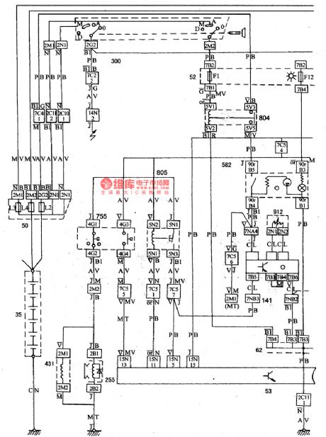
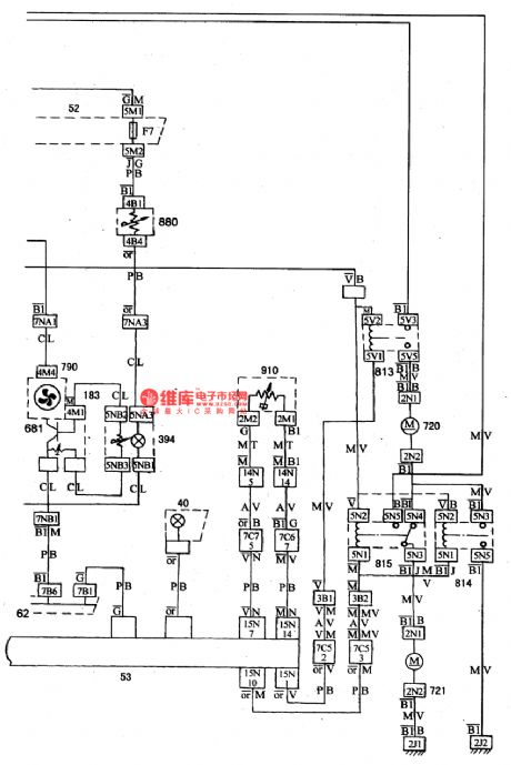
Figure 1-a the principle air-conditioning circuit of DPCA-VOLCANE DC714OZX53-water temperature controller; 141-air-conditioning amplifier; 225-compressor magnetic clutch; 431-idling speed improving magnetic valve; 582-cold air(A/C) switch; 813-fan low-speed relay; 814-fan transmission relay; 912-evaporator temperature sensor; L2-fusible links
Figure 1-b the principle air-conditioning circuit of DPCA-VOLCANE DC714OZX(extend)40h-water warning lamp
(View)
View full Circuit Diagram | Comments | Reading(467)
Double closed loop control of electric bicycle charger circuit principle diagram
Published:2011/6/3 21:44:00 Author:Fiona | Keyword: Double closed loop control, electric bicycle charger
The charger is specifically designed for electric bicycle battery, it rectifys AC then uses IGBT to pressure regulating to achieve the charging voltage that the battery needs is about 3 6 V, control through the voltage and the current double closed loop to achieve the three-stage charging purposes. Chargers mainly consists of the major circuit and control circuit.The circuit principle is shown in the diagram. (View)
View full Circuit Diagram | Comments | Reading(3751)
The micro-resistance test circuit
Published:2011/5/26 22:17:00 Author:Borg | Keyword: micro-resistance, test circuit
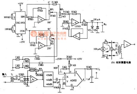
Micro-resistance is tested in the method of 4-terminal measure, i.e the tested resistance Rx is imposed with a AC stable current with the frequency of 1KHZ, the stable current only flow through Rx and it's irrelevant to the cables and touching resistance. Then the voltage between the two terminals of Rx reduces by Ui, which is tested by the sensor so that we know the resistance. The figure (a) is a actual test circuit. OSC-O5X is the 2-phase oscillator of 1KHZX, i.e a oscillator whose phase difference is 90°. The output signal is magnified by A1 and A2, then they are sent out in 4 phases of 0°,90°,180°and 270°.
(View)
View full Circuit Diagram | Comments | Reading(804)
The headlight circuit of Daewoo Racer
Published:2011/5/26 22:05:00 Author:Borg | Keyword: headlight circuit, Daewoo Racer
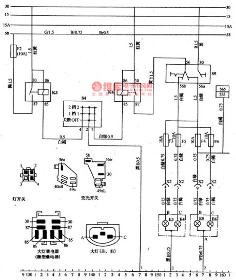
1.see as the figure, all the lights are under the control of switch S4. 0 gear means off. By relay K3, 1 gear connects No.58 circuit: width E7~ElO、E13 and E14, instrument lamps E41~E44, license lamp E11 and El2, glove box lamp E26 and igniter E27 can get through. When it is at 2 , besides the above lamps, it gets through the No.56 circuit by the relay K4, and the headlight is on. The dimmer overtaking switch(s5) can control high beams(E3 and E5) or low beams(E4 and E6), the overtaking signal is delivered by pressing key to get through E3 and E5.
See as the figure. the headlight circuit of Daewoo Racer (View)
View full Circuit Diagram | Comments | Reading(1408)
The wiper and washer circuit of DPCA-VOLCANE DC714OZX
Published:2011/5/19 21:48:00 Author:Borg | Keyword: wiper and washer circuit, DPCA-VOLCANE
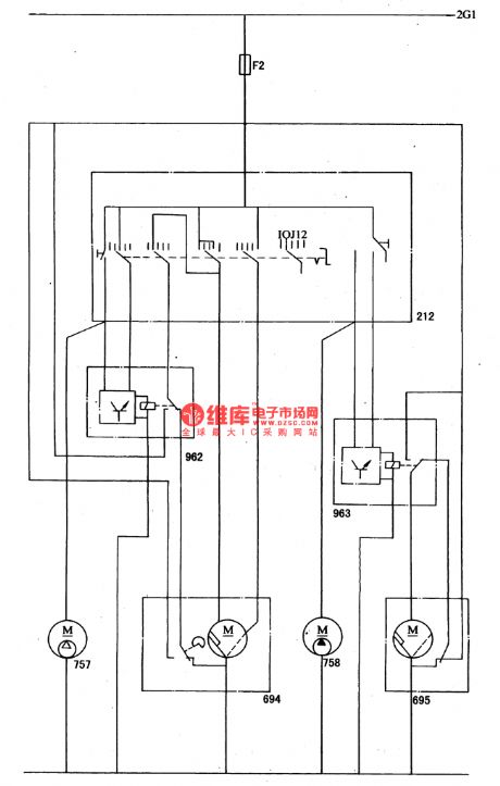
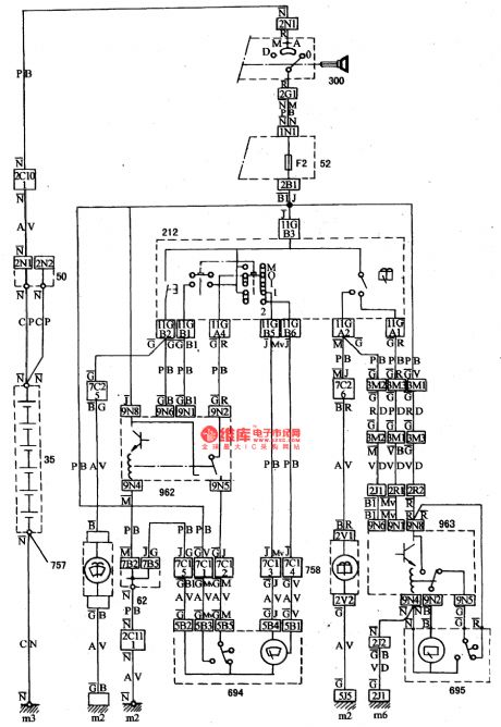
When the igniting switch(300) is normally working, the wire of 2G1 will link to the switch of 212. (Including the fusebox FZ), there are 5 gears in the switch. In the frontend of the marked position in the figure, 1 means stepper gear( single step work ), 0 means stopping working, J means interrupted wiping. The interval relay(962) controlled circuit works when it links to the power supply fire wire, and the wiper motor(694) was controlled by the switch of 212; the interval motor(962) terminal is designed to connect with the fire wire, and the motor wipe 1-2 times at a low speed, then keep still for 6-8s, and wipe again 1-2 times, then keep still for 6-8s```
(View)
View full Circuit Diagram | Comments | Reading(490)
The rotating speed test circuit of photo interrupters
Published:2011/5/26 22:09:00 Author:Borg | Keyword: rotating speed, photo interrupters

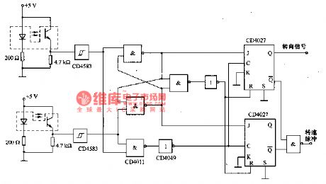
The figure is a rotating speed test circuit of photo interrupters. The circuit is equiped with 2 photo interrupters which are installed in 2 discs with a silt, it can be used to test the rotating speed and steering direction,besides, it canlink CD4027 to corresponding display equipment.
(View)
View full Circuit Diagram | Comments | Reading(1098)
Use common components high-precision polarity conversion circuit
Published:2011/6/3 11:00:00 Author:Fiona | Keyword: Use common components, high-precision, polarity conversion
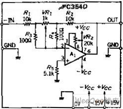
circuit work
Because the OP amp loop gain mainly depends on the ratio of input resistance and the feedback resistance .So resistance has margin of error, the gain will be a corresponding errors.To get more than four-digit precision, we need high-precision resistor. The resistor R3, R4 used to narrow the variable scope of VR1 is 1 / 100 of the R1, R2 resistance, so that you can compensate the deviation of the resistance, in fact,R1 is 9.9 k ohms , R2 is 10.1 k ohms.This worst case is very small, so it is enough that the adjustable range of the VR1 is ± 1%.
Component Selection
(View)
View full Circuit Diagram | Comments | Reading(566)
The current supervision circuit of photocoupler
Published:2011/5/26 22:25:00 Author:Borg | Keyword: supervision circuit, photocoupler
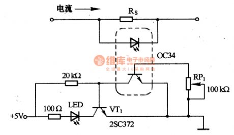
This is a current supervision circuit of photocoupler. In the tested current wires, we put in a resistance of Rs to the test, when the current reaches the regulated value, the voltage on Rs is dropping and the diode in the photocoupler is passable, so the transistor is on, then we cut it offby keeping the grounded potential of VT1 under 0.4V, so the LED is off. When the tested current is dropping, the currents in the diode and transistor of the photocouplerare dropping, so the potential of VT1 rises and it is passable, then the LED is glowing.
(View)
View full Circuit Diagram | Comments | Reading(812)
TDA610Q(ICNBOl) pin functions and data circuit
Published:2011/5/11 2:06:00 Author:TaoXi | Keyword: pin functions, data
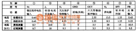
The TDA4605-3 is designed as one kind of switch power supply thick-film integrated circuit that can be used in Philips G8 movement (such as the 25SX8661/93T, 28SX8671/93P), the Goldstar MC-15A movement (CFT一2590), the Dimethoate CT6388M, the Peony 64C2A, T4C2, the Konka F2566E, nlOgE, A1488N, the Changhong NC6 movement (G2966A, G2967A).etc.
The TDA4605-3 has the sampling voltage processing regulator circuit, the under-voltage detection and protection circuit, the excitation pulse output circuit, the soft-start control circuit.etc. This IC is in the 8-pin package, the pin functions and data is as shown in table 16.
Table 16 The pin functions and data of the TDA4605-3
(View)
View full Circuit Diagram | Comments | Reading(1328)
The burglar-alarm system circuit of LED
Published:2011/5/26 22:31:00 Author:Borg | Keyword: burglar-alarm system, LED
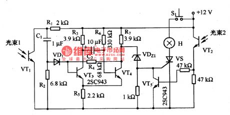
This is a burglar-alarm system circuit of LED. To enlarge the alarm range, the circuit is installed with two LED as the light receiver. The light resource is a infrared ray LED, to reduce the interruption from other rays, it needs to modulate the LED ray. If the beam of the LED is shadowed, the NPN of VTI stops work, and CI generates electricity through VD1, and the base electrode of VT3 is provided with current and VT3 is passable. In the meantime, the single stable circuit consisting of VT3 and VT4 is in a temporarily stable state.
(View)
View full Circuit Diagram | Comments | Reading(1064)
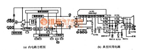
TDA610lQ integrated block internal box circuit
Published:2011/5/11 2:10:00 Author:TaoXi | Keyword: integrated block, internal box
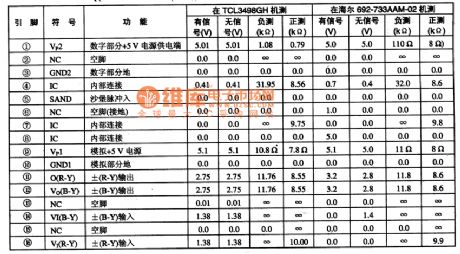
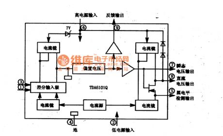
The TDA4665 and TDA4665T are designed as the baseband delay IC that is produced by the PHILIPS company, and it can be used in a variety of domestic multi-system TVs.
The TDA4665 and TDA4665T use the switch capacitor technology, there are two filters to do one line time delay (64 us). The integrated block internal box circuit and the typical application in Haier 692-733AA TV are as shown in figure 12. This IC is in the 16-pin DP DIP package or 16-pin scaled type flat package, the pin functions and data of this circuitare as shown in table 15.
(View)
View full Circuit Diagram | Comments | Reading(869)
The LEV evaluation circuit of μA741
Published:2011/5/26 23:10:00 Author:Borg | Keyword: LEV, evaluation circuit
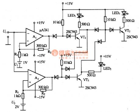
This is a LEV evaluation circuit of μA741. When the input signal Ui is lower than IV, the LED1 is glowing; when the signal ranges 1~2V, the LED2 is glowing; when the signal is higher than 2V, the LED3 is glowing. As the circuitis installed with a calculating amplifier, so we can briefly evaluate the LED of weak signals. The reference voltage of U1 and U2 is provided by a voltage-steady diode. The EH of non-sensitive area is computed in the following way, i.eIn the formula, HOU and UOL are the maximum positive and negative voltages respectively of the computing amplifiers of A1 and A2.
(View)
View full Circuit Diagram | Comments | Reading(977)
555 high-performance streetlights photoelectric control circuit
Published:2011/6/2 18:47:00 Author:TaoXi | Keyword: high-performance, streetlights, photoelectric control
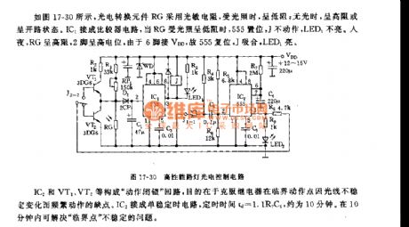
As the figure 17-30 shows, the photoelectric conversion element RG uses the photoresistor, when there is the light, it has the low resistance; when there is no light, it has the high resistance or in the open state. IC1 is the comparator circuit, when RG is lighted and has the low resistance, 555 sets, Jwillnotact, LED1 turns off. At night, RG has the high resistance, pin-2 has the high electric potential, because pin-6 connects with VDD, so 555 resets, J closes and LED1 turns on.
The action locking loop is composed of the IC2 and VT1,VT2. IC2 is the monostable timing circuit, the timing time td=1.1R7C6, it is about 10 minutes.
(View)
View full Circuit Diagram | Comments | Reading(509)
555 writing table lamp timing control circuit
Published:2011/5/23 1:42:00 Author:TaoXi | Keyword: writing, table lamp, timing control
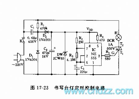
As the figure 17-23 shows, the control circuit is composed of the capacitor step-down rectifier circuit, the low-frequency oscillator circuit and the control circuit. This circuit can automaticly control the light toturn on for 50 minutes and turn off for 10 minutes, then turns on again, so it can protect your eyesight and health.
The astable multivibrator is composed of the 555 and the R2,R3,C3, the oscillation frequency f=1.44/(R2+2R3)C3, the capacitor C3's charging time t=1.1(R2+R3)C3, the discharging time t=1.1R3C3. The pin-5 of control port connects to the VDD to improve pin-6's threshold level.
(View)
View full Circuit Diagram | Comments | Reading(649)
The trigger timing circuit of LED
Published:2011/5/23 2:09:00 Author:Borg | Keyword: trigger timing circuit, LED
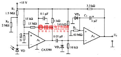
This is a trigger timing circuit of LED. In the circuit, A1 is the comparator, A2 is the single trigger timer. When the light obstructed, the current in VD, the LED, is changing, and the current is output by A1 then it triggers A2,then A2 converts the current into a low LEV and keep it for 60S(it is decided by R3 and CI). The sensitivity to the light of VD can be changed by the resistances of R1 and R2, but the ratio between the two resistance values is stable, so that VD could be provided with a certain reverse bias voltage.
(View)
View full Circuit Diagram | Comments | Reading(647)
555 aphonia throat alternative device circuit
Published:2011/5/25 1:02:00 Author:TaoXi | Keyword: aphonia, throat, alternative device
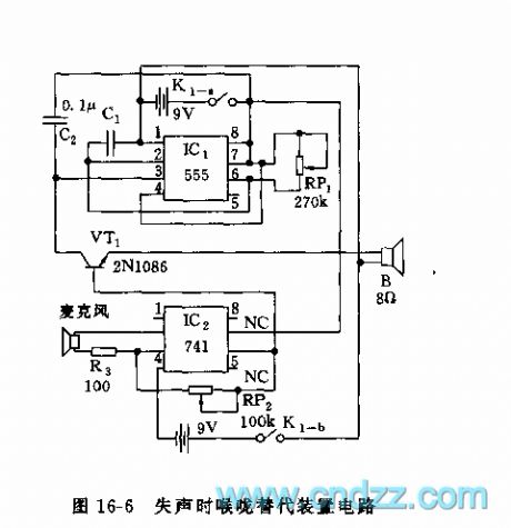
The IC2(uA741) is designed as the voice amplifier, the amplification number depends on the value of RP2/R3, the maximum is 1000 times. The microphone picks up the throat voice and this throat voice is amplified by the IC2, then adds to VT1. The tone generator is composed of the IC1(555) and RP1, C1, C2, it's output pulse (pin-3) is changed into the triangular wave by C2 and RP1, so it produces the modulation to 555 oscillator to drive the speaker to send out the variable-tones sound waves. This device also can be used in the applications of analog dubbing and the analog tone voice.
(View)
View full Circuit Diagram | Comments | Reading(1308)
555 gradually ringing type sleep wake-up device circuit
Published:2011/5/24 22:56:00 Author:TaoXi | Keyword: gradually, ringing, sleep, wake-up
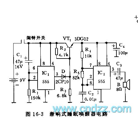
As the figure 16-3 shows, the delay switch circuit is composed of the IC1 and the R1,C1, the 800Hz multivibrator is composed of the IC2 and R4,R5,C2. When the electric clock's timing contact points turn on the power supply of this circuit,and thecapacitor C1's voltage can not be mutated, so pin-2 of 555 has the high electrical level. At this time, the 555's output port has the low electrical level, the diode D cuts off. When the electric potential of IC1's pin-2 and pin-6 drops to 1/3VDD, the circuit reverses, and the pin-3 has the high electrical level, this charging delay time is about 8 seconds. Then D conducts, the b electrode's potential of the VT1 tube increases.
(View)
View full Circuit Diagram | Comments | Reading(647)
The rotating speed test circuit formed by NE555 and so on
Published:2011/5/26 23:18:00 Author:Borg | Keyword: rotating speed, test circuit
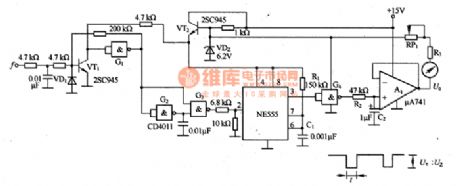
The input frequecy is a responding signal to rotating speed. The signal is shaped by the Schmidt trigger circuit which is formed by VT1 and G1, and then is differentiated by G2 and G3, then the pulse signal triggers the signle-stable multivibrator which consists of NE555. The 3-lead output comes across G4, and then runs through R2 and C2 to be integrated, finally comes across A1 buffer and comes out from the drive meter. At the same time, the output pulse width of G4 is t, amplitude is Ue, frequency is (equal to the frequency of input signals), and the output voltage of A1 is U.
(View)
View full Circuit Diagram | Comments | Reading(818)
automatic battery charger circuit of intelligent pulse electric bicycle
Published:2011/5/30 21:00:00 Author:Fiona | Keyword: automatic battery charger, intelligent pulse electric bicycle
(View)
View full Circuit Diagram | Comments | Reading(3423)
555 simple sickbed calling device circuit
Published:2011/5/25 1:35:00 Author:TaoXi | Keyword: simple sickbed, calling device
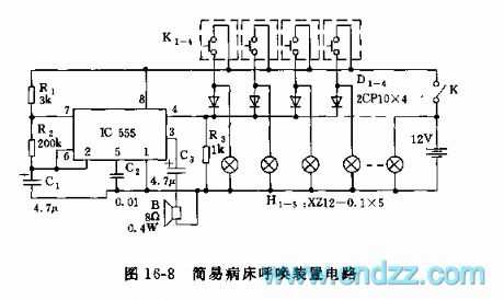
As the figure 16-8 shows, the controllable multivibrator is composed of the 555 and R1,R2,C1, the circuit start-up depends on the electric potential of the reset port pin-4. Whenyou press any one swith of the K1~K4, pin-4 has the high electric potential, 555 starts working to send out the sound and light alarm signals. The oscillation frequency f=1.44/(R1+2R2)C1, it is about 1000Hz.
(View)
View full Circuit Diagram | Comments | Reading(576)
| Pages:1767/2234 At 2017611762176317641765176617671768176917701771177217731774177517761777177817791780Under 20 |
Circuit Categories
power supply circuit
Amplifier Circuit
Basic Circuit
LED and Light Circuit
Sensor Circuit
Signal Processing
Electrical Equipment Circuit
Control Circuit
Remote Control Circuit
A/D-D/A Converter Circuit
Audio Circuit
Measuring and Test Circuit
Communication Circuit
Computer-Related Circuit
555 Circuit
Automotive Circuit
Repairing Circuit