
Electrical Equipment Circuit
Index 77
WIDEBAND_HIGH_CREST_FACTOR_RMS_TO_DE_COMVERTER
Published:2009/6/25 2:26:00 Author:Jessie
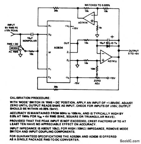
View full Circuit Diagram | Comments | Reading(1587)
POWER_VOLTAGE_TO_CURRENT_CONVERTER
Published:2009/6/25 2:17:00 Author:Jessie
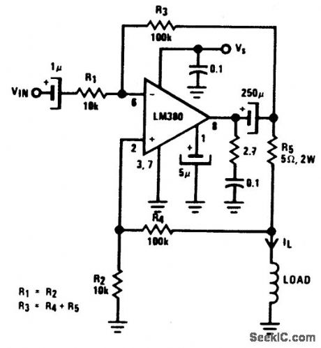
Low cost converter is capable of supplying constant ac currents up to 1 A over variable loads. (View)
View full Circuit Diagram | Comments | Reading(1317)
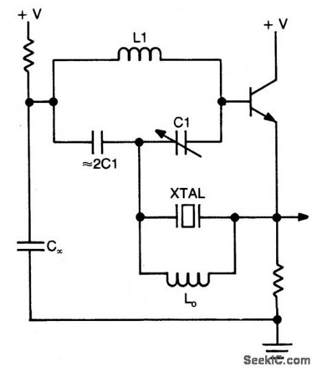
BUTLER_COMMON_BASE_OSCILLATOR_BASIC_CIRCUIT
Published:2009/6/25 2:17:00 Author:Jessie
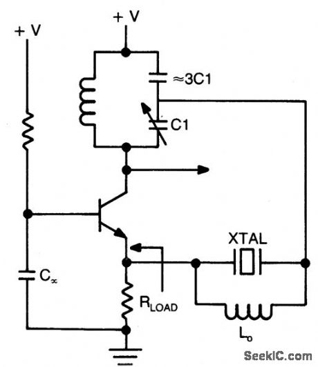
Circuit Notes This circuit operates at or near series resonance. It has fair to poor circuit design with parasitics, touch to tune, and fair frequency stability. (View)
View full Circuit Diagram | Comments | Reading(1626)
CALCULATOR_TO_STOPWATCH_CONVERTER
Published:2009/6/25 2:17:00 Author:Jessie
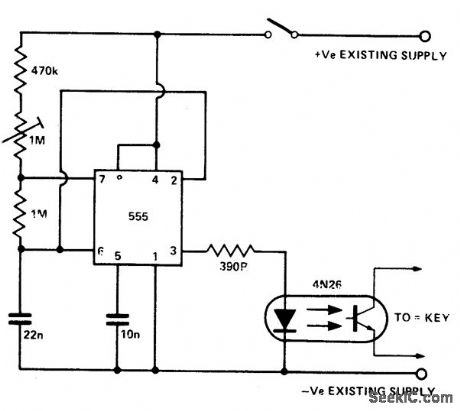
This circuit can be fitted to any calculator existing with an automatic constant to enable it to be used as a stop-watch. The 555 timer is set to run at a suitable frequency and connected to the existing calculator battery via the push-on push-off switch and the existing calculator on-off switch. (View)
View full Circuit Diagram | Comments | Reading(2851)
BUTLER_EMITTER_FOLLOWER_OSCILLATOR_BASIC_CIRCUIT
Published:2009/6/25 2:16:00 Author:Jessie
Circuit Notes
This circuit operates at or near series resonance. It is a good circuit design with no parasitics. It is easy to tune with good fre-quency stability. (View)
View full Circuit Diagram | Comments | Reading(689)
COLPITTS_HARMONIC_OSCILLATOR(BASIC_CIRCUIT)
Published:2009/6/25 2:14:00 Author:Jessie
Circuit NotesThis circuit operates 30-200 ppm above series resonance. Physically simple, but analytically complex. It is inexpensive with fair frequency stability. (View)
View full Circuit Diagram | Comments | Reading(1405)
BUTLER_EMITTER_FOLLOWER_OSCILLATOR(100_MHz)
Published:2009/6/25 2:13:00 Author:Jessie
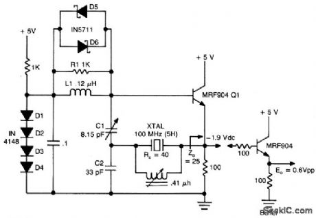
Circuit NotesThis circuit has good performance without any parasitics because emitter follower amplifier has a gain of only one with built-in negative feedback to stabilize its gain. (View)
View full Circuit Diagram | Comments | Reading(0)
CURRENT_TO_VOLTAGE_CONVERTER
Published:2009/6/25 2:12:00 Author:Jessie
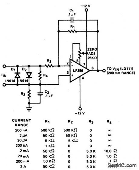
Converter features eight decades of cur-rent range. The circuit is intended to be used with the 200.0 mV range of a DVM. (View)
View full Circuit Diagram | Comments | Reading(2914)
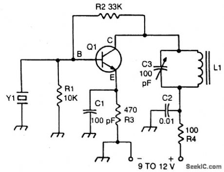
PIERCE_HARMONIC_OSCILLATOR20_MHz
Published:2009/6/25 1:57:00 Author:Jessie
Circuit NotesThis circuit has excellent short term frequency stability because the external load tied across the crystal is mostly capacitive rather than resistive, giving the crystal a high in-circuit Q. (View)
View full Circuit Diagram | Comments | Reading(659)
COMPARATOR
Published:2009/6/25 1:56:00 Author:Jessie
An operational amplifier is used as a comparator which is capable of driving approximately 10 logic gates. (View)
View full Circuit Diagram | Comments | Reading(0)
COMPARATOR_WITH_HYSTERESIS
Published:2009/6/25 1:55:00 Author:Jessie
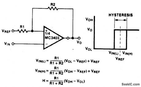
View full Circuit Diagram | Comments | Reading(1429)
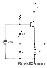
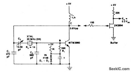
CRYSTAL_CONTROLLED_TRANSISTOR_OSCILLATOR_
Published:2009/6/25 1:54:00 Author:Jessie
View full Circuit Diagram | Comments | Reading(621)
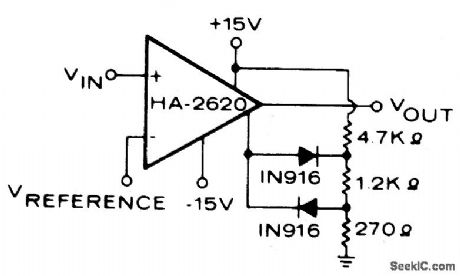
HIGH_IMPEDANCE_COMPARATOR
Published:2009/6/25 1:54:00 Author:Jessie
View full Circuit Diagram | Comments | Reading(609)
PRECISION_DUAL_LIMIT_GO_NO_GO_TESTER
Published:2009/6/25 1:53:00 Author:Jessie
View full Circuit Diagram | Comments | Reading(1083)
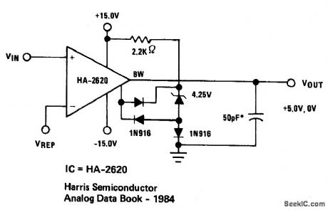
LIMIT_COMPARATOR_1
Published:2009/6/25 1:51:00 Author:Jessie
View full Circuit Diagram | Comments | Reading(0)
TEMPERATURE_COMPENSATED_CRYSTAL_OSCILLATOR
Published:2009/6/25 1:51:00 Author:Jessie
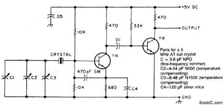
Circuit NotesTwo different negative-coefficient capacitors change in capacitance to counteract or compensate are blended to produce the desired for the decrease in frequency of the normal AT-cut characteristics. (View)
View full Circuit Diagram | Comments | Reading(0)
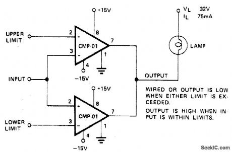
WINDOW_COMPARATOR_DRIVING_HIGH_LOW_LAMPS
Published:2009/6/25 1:40:00 Author:Jessie
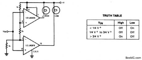
View full Circuit Diagram | Comments | Reading(0)
HIGH_POWER_CONTROLFOR_SENSITIVE_CONTACTS
Published:2009/6/25 1:40:00 Author:Jessie
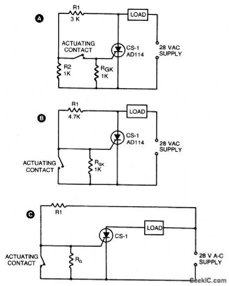
Two simple arrangements for resistive loads are shown in A & B. The circuit in A will provide load power when the actuating contact is closed, and no power when the contact is open. B provides the reierse of this action-power being supplied to the load when the contact is open with no load power when the contact is closed. If desired, both circuits can be made to latch by operating with dc instead of the indicated ac supply. In both of these circuits, voltage across the sensitive contacts is under 5 volts, and contact current is below 5 mA. For inductive loads, R1 would normally be returned to the opposite side of the load as shown in C. (View)
View full Circuit Diagram | Comments | Reading(0)
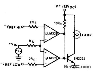
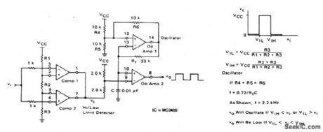
WINDOW_COMPARATOR
Published:2009/6/25 1:39:00 Author:Jessie

This circuit gives an output (which in this case is 0V) when an input voltage lies in be-tween two specified voltages. When it is out-side this window, the output is positive. The two op amps are used as voltage comparators. When Vin is more positive than Vref (upper) the output of IC1 is positive and Dl is forward biased. Otherwise the output is negative, D1 reverse biased and hence Vout is 0V. Similarly, when Vin is more negative than Vref (lower), the output of IC2 is positive; D2 is forward biased and this Vout is positive. Otherwise Vout is 0V. When Vin lies within the window set by the reference voltages, Vout is 0V. (View)
View full Circuit Diagram | Comments | Reading(0)
HIGH_LOW_LIMIT_ALARM
Published:2009/6/25 1:38:00 Author:Jessie
View full Circuit Diagram | Comments | Reading(1284)
| Pages:77/126 At 206162636465666768697071727374757677787980Under 20 |
Circuit Categories
power supply circuit
Amplifier Circuit
Basic Circuit
LED and Light Circuit
Sensor Circuit
Signal Processing
Electrical Equipment Circuit
Control Circuit
Remote Control Circuit
A/D-D/A Converter Circuit
Audio Circuit
Measuring and Test Circuit
Communication Circuit
Computer-Related Circuit
555 Circuit
Automotive Circuit
Repairing Circuit