
Electrical Equipment Circuit
Index 71
IC_function_generator_connected_for_FSK_frequency_shift_keying
Published:2009/7/25 4:00:00 Author:Jessie
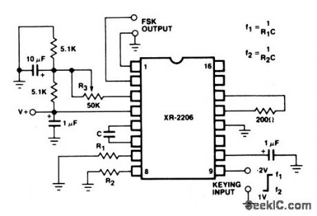
This circuit is similar to that of Fig. 5-31, except that the XR-2206 is connected for sine FSK outputs. Mark and space frequencies f1 and f2 are selected by the choice of R1, R2, and C, as shown by the equation. The output is phase-continuous during transitions. The keying signal is applied at pin 9. The circuit can be converted to split-supply operation by replacing ground with V-.R3 sets the FSK output amplitude. (View)
View full Circuit Diagram | Comments | Reading(2341)
IC_function_generator_connected_for_sine_output_with_external_adjustment
Published:2009/7/25 3:59:00 Author:Jessie
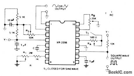
This circuit is similar to that of Figs. 5-31/5-32, except that the harmonic content of the sine output can be reduced to about 0.5%. Set RB at midpoint and adjust RA for minimum distortion. With RA set, adjust RB to further reduce distortion. If a triangle output is desired, open S1. (View)
View full Circuit Diagram | Comments | Reading(782)
Voltage_controlled_oscillator_single_supply
Published:2009/7/25 4:40:00 Author:Jessie
This circuit shows the basic connection for an XR-2207 connected for single-supply operation .The functions and electrical characteristics are as shown in Figs. 5-52B and 5-52C. (View)
View full Circuit Diagram | Comments | Reading(709)
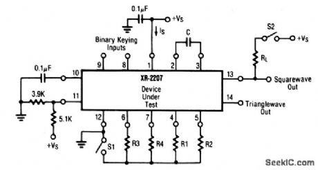
Voltage_controlled_oscillator_split_supply
Published:2009/7/25 4:36:00 Author:Jessie

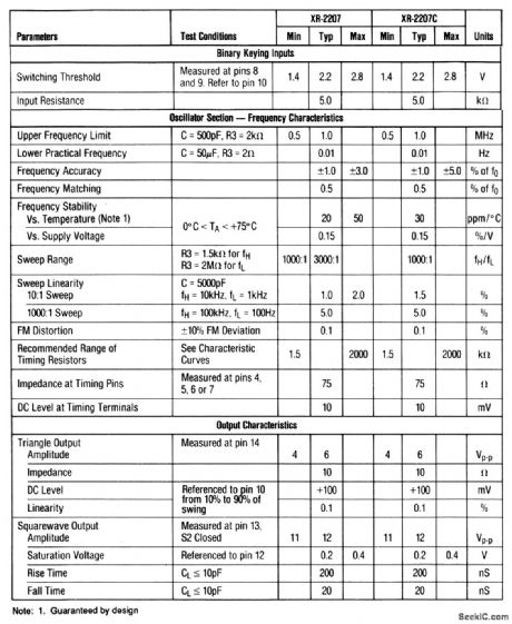
This circuit shows the baisc connection for an XR-2207 connected for split-supply operation. The output frequency(both sine and triangle) is controlled by C (pin2/3)and R1 through R4 .If a single timing resistors is used, the frequency is 1/RC. Otherwise ,the frequency is either 1/(R1//R2)C or 1/(R1//R4)C. Timing resistors R1 through R4 are activated by the logic signals at the binary keying input (pin 8/9),as shown in Fig,5-52B.Figure 5-52C shows the electrical characteristics. (View)
View full Circuit Diagram | Comments | Reading(796)
33_V_5_V_and_12_V_from_six_to_twelve_cells
Published:2009/7/25 4:29:00 Author:Jessie
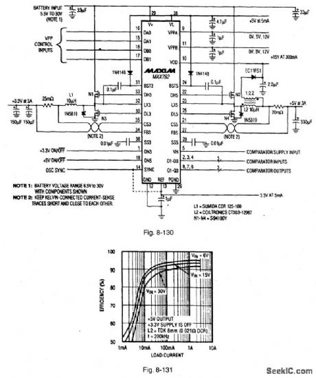
Figttre 8-130 shows a MAX782 notebook SMPS connected to provide 3.3 V, 5 V, and 12 V from six to twelve battery cells. Figure 8-131 shows the efficiency curves. The input voltage range is 5.5 V to 30 V, quiescent current (VIN = 15 V) is 420 μA, maximum load current (5-V output, VIN = 6) and 3.3-V output, VIN = 6 V) is 3 A, and the shutdown current is 70 μA. An evaluation kit is available from Maxim. MAXIM BATTERY MANAGEMENT CIRCUIT COLLECTION, 1994, P. 37. (View)
View full Circuit Diagram | Comments | Reading(555)
System_voltage_monitor
Published:2009/7/25 4:26:00 Author:Jessie
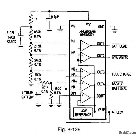
Figure 8-129 shows a MAX8214 voltage monitor connected to monitor the condition of a six-cell NiCad stack and a lithium backup battery. Larger portable systems often require several voltage-monitoring comparators to detect the status of main and backup batteries, as well as for power-fail monitoring and ac adapter detection. This circuit performs such monitoring and draws only 3 μA per comparator. The input-voltage range for the monitored voltage is 1.25 V to 100 V, and 2.7 V to 11 V for the IC. Quiescent current (VIN = 5 V) is 16 μA, and threshold accuracy is 11% maximum. When the NiCad stack is fully charged, output 3 goes high. When the NiCad stack voltage drops to a low (but still usable) level, output 2 goes low. When the NiCad stack is dead, output 1 goes low. Output 4 goes low when the lithium battery is dead. MAXIM BATTERY MANAGEMENT CIRCUIT COLLECTION, 1994, P. 77. (View)
View full Circuit Diagram | Comments | Reading(746)
Complete_function_generator
Published:2009/7/25 4:25:00 Author:Jessie
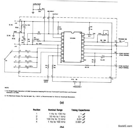
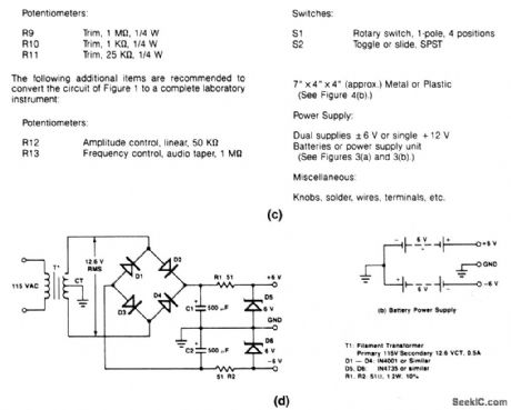
This circuit uses an XR-2206 to provide sine, triangle, and square outputs that can be AM/FM modulated. There are four overlapping frequency ranges selected by S1, as shown in Fig. 5-51B. The parts list, and a typical power supply, are shown in Figs. 5-51C and 5-51D respectively. Each tuning range can be varied over a 100:1 range. The sine/triangle output (P) can be varied from 0 to over 6 Vpp and appears as a 600-Ω source at the output terminal. The square-wave output (full M, or half L) is available for scope sync or to drive logic circuits. S1 selects range, S2 selects triangle or sine output, R9 sets dc-offset level of the triangle or sine output, R10 is adjusted for minimum harmonic content of the sine output. R11 is adjusted for optimum symmetry of the sine output. R12 sets the amplitude of the triangle/sine output, and should be a front-panel control, as should R13, which varies the frequency over the 100:1 range. To adjust for minimum distortion, monitor the output at P with S2 closed. Set R12 for a non-clipping maximum swing, then adjust R10 and R11 alternately for minimum distortion. Use a distortion meter, if desired, for final adjustment. Typical distortion is less than 1% from 1 Hz to 10 kHz, and less than 3% over the entire range. (View)
View full Circuit Diagram | Comments | Reading(3060)
High_side_current_sense_amplifier
Published:2009/7/25 4:25:00 Author:Jessie
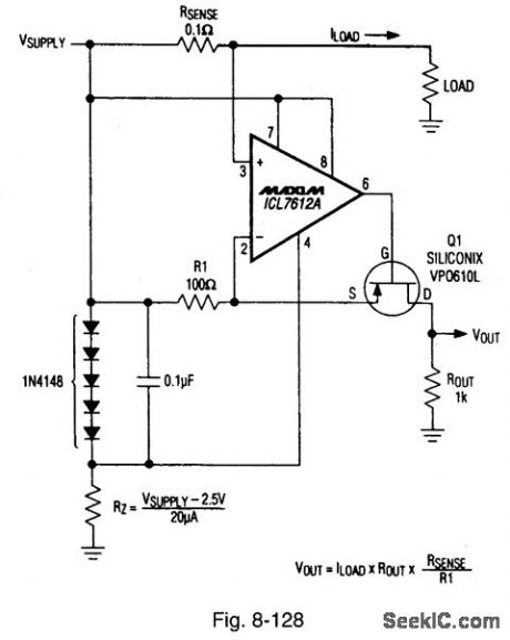
Figure 8-128 shows an ICL7612A micropower op amp connected to provide sensing of high-side current. The operating voltage range is 4.5 V to 48 V, quiescent current (VIN = 5 V) is 20 μA, and the gain factor is 1 VA. The circuit senses current in the positive battery lead, allowing the battery's negative terminal to be directly connected to circuit ground. The circuit output is a ground-referenced output voltage that is directly proportional to the current flowing in the low-value sense resistor. The output is typically added to the input of an A/D converter or integrating V/F converter. Because the output current is a true-current source, the output can be referenced to any level within the supply limits. The value of R1 should be kept in the range of 100 × RSENSE to 1000× RSENSE. MAXIM BATTERY MANAGEMENT CIRCUIT COLLECTION, 1994, P. 75.
(View)
View full Circuit Diagram | Comments | Reading(1282)
IC_rprecision_waveform_generator_with_sweep_and_frequency_modulation_
Published:2009/7/25 4:23:00 Author:Jessie
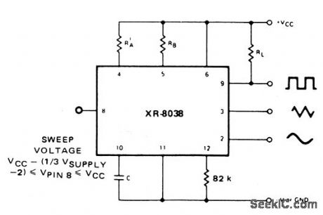
These circuits are similar to that of Fig. 5-47, except that the circuits provide for FM or sweep modulation. Use circuit 5-50A for FM (small deviations, about±10%). Use circuit 5-50B for a sweep range of 1000:1. As a guideline, the sweep frequency approaches 0 Hz when the voltage at pin 8 equals VCC, and reaches maximum at the lower pin-8 voltage limit of VCC - (1/3 VSUPPLY -2).Waveform symmetry variations can be minimized when a 10-M resistor is added between pins 5 and 11. (View)
View full Circuit Diagram | Comments | Reading(3240)
IC_precision_waveform_generator_with_minimum_sine_wave_distortion
Published:2009/7/25 4:22:00 Author:Jessie
This circuit is similar to that of Fig. 5-47, except that sine-wave distortion can be adjusted to less than 0.5%. (View)
View full Circuit Diagram | Comments | Reading(1231)
Voltage_controlled_oscillator_frequency_sweep_operation
Published:2009/7/25 4:46:00 Author:Jessie
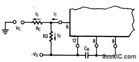
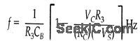

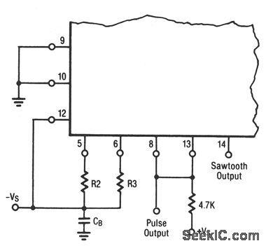
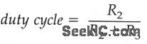

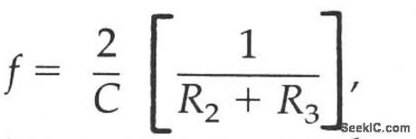
This circuit shows the connections required to convert the circuits of Figs. 5-52 and 5-53 to pulse and sawtooth operation. The duty cycle of the output waveforms is given as:and can be varied from 0.1% to 99.9% by proper choice of timing resistors. The frequency of oscillation is given as:
and can be modulated or swept by connecting R2 and R3 to common control voltage Vc instead of -Vs. (View)
View full Circuit Diagram | Comments | Reading(868)
LED_BAR_PEAK_PROGRAM_METER_DISPLAY_FOR_AUDIO
Published:2009/6/28 21:39:00 Author:Jessie

Circuit NotesA bar column of LEDs is arranged so that as the audio signal level increases, more LEDs in the column light up. The LEDs are arranged vertically in 6 dB steps. A fast response time and a one second decay time give an accurate response to transients and a low flicker decay characteristic. On each of the op amps inverting inputs is a dc reference voltage, which increases in 6 dB steps. All noninverting inputs are tied together and connected to the positive peak envelope ofthe audio signal.hus, as this envelope exceeds a particular voltage reference, the op amp output goes high and the LED lights up. Also, all the LEDs below this are illuminated. (View)
View full Circuit Diagram | Comments | Reading(816)
60_MHz_POWER_GAIN_TEST_CIRCUIT
Published:2009/6/28 21:09:00 Author:Jessie
View full Circuit Diagram | Comments | Reading(1162)
POWER_METER(1_kW_FULL_SCALE)
Published:2009/6/28 21:09:00 Author:Jessie
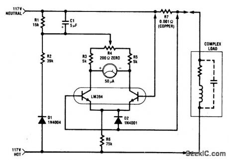
The circuit is intended for 117 Vac ±50 Vac operation, but can be easily modified for higher or lower voltages. It measures true (nonreactive) power be ing delivered to the load and requires no external power supply. Idling power drain is only 0.5 W. Load current sensing voltage is only 10 mV, keeping load voltage loss to 0.01%. Rejection of reactive load currents is better than 100:1 for linear loads. Nonlinearity is about 1% full scale when using a 50 μA meter movement. (View)
View full Circuit Diagram | Comments | Reading(1294)
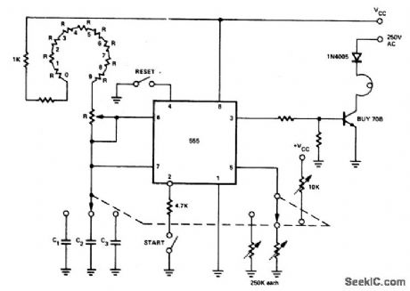
PHOTOGRAPHIC_TIMER
Published:2009/6/28 21:04:00 Author:Jessie
View full Circuit Diagram | Comments | Reading(1265)
SHUTTER_TESTER
Published:2009/6/28 21:03:00 Author:Jessie
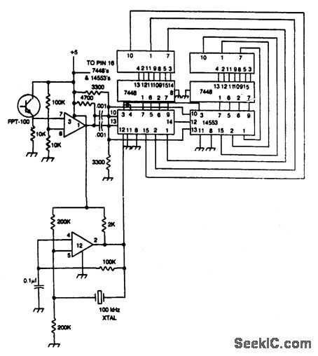
Shutter speed tester combines frequency counter, crystal oscillator, and photo-transistor-operated gate generator. Oscillator pulses are counted as long as the shutter is open. Reset is automatic at the instant the shutter opens.
(View)
View full Circuit Diagram | Comments | Reading(2317)
FLASH_EXPOSURE_METER
Published:2009/6/28 21:02:00 Author:Jessie
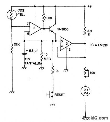
Strobe light meter catches the peak of flash intensity and holds it long enough to give a reading. The reset button must be pressed before each measurement. (View)
View full Circuit Diagram | Comments | Reading(1728)
REMOTE_FLASH_TRIGGER
Published:2009/6/28 21:01:00 Author:Jessie

Transistor Q1 is a light-activated silicon-controlled rectifier (LASCR). The gate is tripped by light entering a small lens built into the top cap. To operate, provide a 6-in. length of stiff wire for the anode and cathode connections and terminate the wires in a polarized power plug that matches the sync terminals on your electronic flashgun (strobelight). Make certain the anode lead connects to the positive sync terminal. When using the device, bend the connecting wires so the LASCR lens faces the main flash. This will fire the remote unit. (View)
View full Circuit Diagram | Comments | Reading(1740)
FLASH_SLAVE_DRIVER
Published:2009/6/28 20:58:00 Author:Jessie
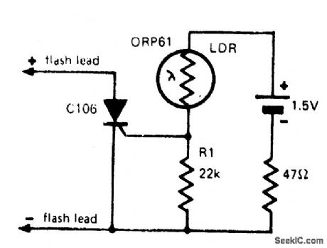
In photography, a separate flash, triggered by the light of a master flash light, is often required to provide more light, fill-in shadows etc. The sensitivity of this circuit depends on the proximity of the master flash and the value of R1. Increasing R1 gives increased sensitivity. (View)
View full Circuit Diagram | Comments | Reading(0)
SOUND_ACTIVATED_STROBE_TRIP
Published:2009/6/28 20:57:00 Author:Jessie
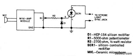
Take strobe-flash pictures the instant a pin pricks a balloon, a hammer breaks a lamp bulb or a bullet leaves a gun. Use a transistor amplifier of 1-watt rating or less. (It must have an output transformer.) The amplifier is terminated with a resistor on its highest output impedance, preferably 16 ohms. To test, darken room lights, open camera shutter, and break a lamp bulb with a hammer. The sound of the hammer striking the lamp will trigger the flash, and the picture will have been taken at that instant. (View)
View full Circuit Diagram | Comments | Reading(1499)
| Pages:71/126 At 206162636465666768697071727374757677787980Under 20 |
Circuit Categories
power supply circuit
Amplifier Circuit
Basic Circuit
LED and Light Circuit
Sensor Circuit
Signal Processing
Electrical Equipment Circuit
Control Circuit
Remote Control Circuit
A/D-D/A Converter Circuit
Audio Circuit
Measuring and Test Circuit
Communication Circuit
Computer-Related Circuit
555 Circuit
Automotive Circuit
Repairing Circuit