
Electrical Equipment Circuit
Index 78
REMOTE_CONTROL_FOR_LAMP_OR_APPLIANCE
Published:2009/6/25 1:38:00 Author:Jessie
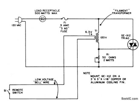
The circuit uses the primary current of a small6.3 volt filament transformer to actuate a triac and energize the load. When switch S1, in the six-volt secondary, of the transformer is open, a small magnetizing current flows through the primary winding. This magnetizing current may be large enough to trigger the triac. Therefore, a shunting resistor, R1, is required to prevent such triggering. R1, is adjusted for the highest resistance that will not cause the triac to trigger with S1 open. When single-pole remote switch, S1, closes, the secondary of the transformer is shorted and a high current flows through the 120-volt primary.This triggers the triac and energizes the load.When the triac conducts, current through the primary stops and thus prevents burning out the transformer. (View)
View full Circuit Diagram | Comments | Reading(1631)
DUAL_LIMIT_COMPARATOR
Published:2009/6/25 1:37:00 Author:Jessie
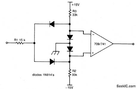
This circuit gives a positive output when the input voltage exceeds 8.5 volts. Between these limits the output is negative. The posi-tive limit point is determined by the ratio of R1, R2, and the negative point by R1, R3. The forward voltage drop across the diodes must be allowed for. The output may be inverted by reversing the inputs to the op amp. The 709 is used without frequency compensation. (View)
View full Circuit Diagram | Comments | Reading(0)
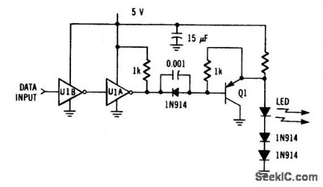
DIODE_FEEDBACK_COMPARATOR
Published:2009/6/25 1:34:00 Author:Jessie
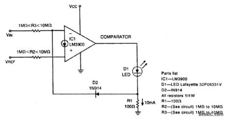
This circuit can drive an LED display with constant current independently of wide power supply voltage changes. It can operate with a power supply range of at least 4V to 30V. With 10M resistances for R2 and R3 and the inverting input of the comparator grounded, the cir-cuit becomes an LED driver with very high input impedance. The circuit can also be used in many other applications where a controllable constant current source is needed. (View)
View full Circuit Diagram | Comments | Reading(0)
COMPARATOR_WITH_VARIABLE_HYSTERESIS_WITHOUT_SHIFTING_INITIAL_TRIP_POINT
Published:2009/6/25 1:34:00 Author:Jessie
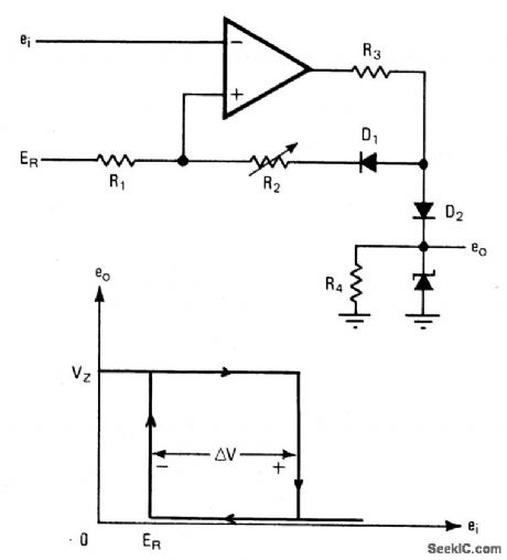
An operational amplifier can be used as a convenient device for analog comparator appli-cations that require two different trip points. The addition of a positive-feedback network introduces a precise variable hysteresis into the usual comparator switching action. Such feedback develops two comparator trip points centered about the initial trip point or refer-ence point. The voltage difference, AY, be-tween the trip points can be adjusted by varying resistor R2. When the output voltage is taken from the zener diode, as shown, it switches between zero and Vz, the zener voltage. (View)
View full Circuit Diagram | Comments | Reading(0)
OPTICAL_TRANSMITTER
Published:2009/6/24 23:43:00 Author:Jessie
Driver circuit uses an MC74LS04 and one discrete transistor. The circuit can drive the LED (MFOE1200) at up to 1 Mbps data rate. (View)
View full Circuit Diagram | Comments | Reading(1531)
PIEZO_DRIVER
Published:2009/6/24 23:42:00 Author:Jessie
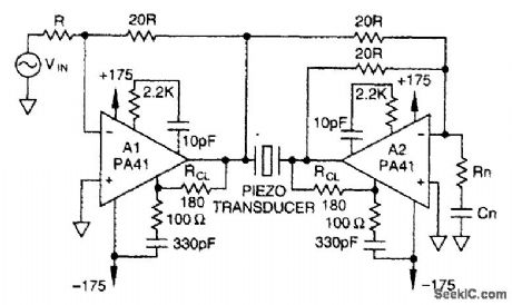
Using a PA41 from Apex Microtechnology, this monolithic amplifier is capable of 350-V operation and delivers 660 V p-p in a bridge circuit. (View)
View full Circuit Diagram | Comments | Reading(0)
PHOTOCELL_MEMORY_SWITCH_FOR_AC_POWER_CONTROL
Published:2009/6/24 23:42:00 Author:Jessie
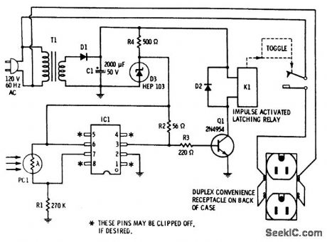
Provides remote control for ac-powered devices by using the beam of a flashlight as a magic wand. The important aspect of this gadget is that it remembers. Activate it once to apply power to a device and it stays on. Activate it a second time and power goes off and stays off. It consists of a combination of a high-sensitivity photocell, a highgain IC Schmitt trigger, and an impulse-actuated latching relay. (View)
View full Circuit Diagram | Comments | Reading(1507)
CMOS_PIEZO_DRIVER_USING_4049
Published:2009/6/24 23:41:00 Author:Jessie

This circuit uses a 4049 IC to drive a 2N2222 switching transistor The transistor drives crysbal 1 a ptezo transducer. (View)
View full Circuit Diagram | Comments | Reading(0)
CMOS_PIEZO_DRIVER
Published:2009/6/24 23:39:00 Author:Jessie

A CMOS-gate and transistor buffer can be used as an effective driver for a piezoelectric transducer. (View)
View full Circuit Diagram | Comments | Reading(0)
ENLARGER_EXPOSURE_METER
Published:2009/6/24 23:36:00 Author:Jessie
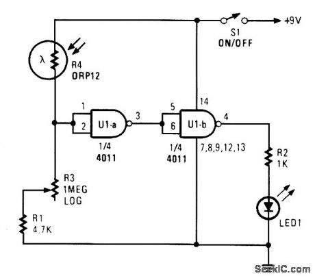
Two gates of a 4011 are used as a comparator. When the resistance of R4 decreases the voltage at pin 1 and 2 increases, producing a logic zero at pin 3, causing pin 4 to go high and activating the LED. R3 is calibrated in light units, or seconds exposure time. To calibrate, set pot R3 so as to just be on the LED ON/OFF threshold. With a light level that is suitable to correctly expose a photographic print, use a known enlarger and a known negative. (View)
View full Circuit Diagram | Comments | Reading(1386)
STROBE_LIGHT
Published:2009/6/24 23:34:00 Author:Jessie

This strobe light operates from standard 120-Vac power,R1 limits the amount of current applied to the voltage doubler stage,which is comprtsed of C1,C2,C3,D1,D2,C4,C5,and C6 Capacitors C1,C2,and C3 are connected in parallel and form a capacitance of 30 μF at 160V. Capacitors C4, C5, and C6 are connected in serles and form an equivalent capacitor of about 53 μF at 480 V . Diodes D1 and D2 not only rectify the ac voltage,but also complete the vltage doubler stage,which convertsthe incoming 120 Vac to the appropriately 300 V that are required by the xenon strobe tube.
The next stage of the circuit is the neon relaxation oscillator and trigger stage This stage is made up of R2, P1,C7,L1,Q1,T1,and T2.As the storage capacitor (made up of C4,C5,and C6) reaches its full-capaclty charge,the voltage divider (made up of R2 and P1) applies voltage to capacitor C7. As C7 charges up,it reaches a threshold voltage level,SCR Q1. When Q1 has a positive pulse on its gate,it fires(causes a short from anode to cathode). That firing action discharges most of the energy stored in C7 into trigger transformers T1 and T2(which have secondaries connected in series to developer 8 kV). The frequency of the 8-kV pulses is determined by the setting of P1 and the value of C7. Because C7 is a fixed capacitor,only the Setting of P1 adjusts the flash rate in this circuit
As soon as an 8-kV pulse is applied from the secondary of T2 (trigger wire) to the trigger lead of FT1,it discharges storage capacitors C4,C5,and C6,which causes it to ionize (flash). The cycle thenrepeats itself until the power is removed from the circuit board by turning off S1 or removing the line cord. (View)
View full Circuit Diagram | Comments | Reading(0)
PHOTO_STROBE_SLAVE_TRIGGER
Published:2009/6/24 23:14:00 Author:Jessie
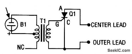
The photo strobe slave trigger circuit uses a solar cell and an SCR to flash any strobe when you trigger your master strobe. The tiny solar cell produces a vet'y small voltage when light falls on its surface. (View)
View full Circuit Diagram | Comments | Reading(1524)
Carrier_System_Transmitter
Published:2009/6/24 23:14:00 Author:Jessie
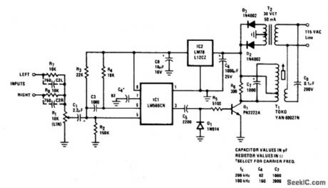
High quality, noise free, wireless FM transmitter/receiver operates over standard power lines. Complete system is suitable for high-quality transmission of speech or music, and will operate from any ac outlet anywhere on a one-acre homesite. Frequency response is 20-20, 000 Hz and THD is under 1/2%. Transmission distance along a power line is at least adequate to include all outlets in and around a suburban home and yard.Two input terminals are provided so that both left and right signals of a stereo set may be combined for mono transmission to a single remote speaker if desired. (View)
View full Circuit Diagram | Comments | Reading(2788)
DARKROOM_TIMER
Published:2009/6/24 23:13:00 Author:Jessie

The electronic darkroom timer is built around a 555 oscillator/timer, a pair of general-purpose transistors, a buzzer, and an LED. The 555 (U1) is configured as an astable multivibrator (free-rututing oscillator). The frequency of the oscillator is determined by the values R1 through R3 and C1 through C4.
Switch S1 is used to divide the capacitor network to vary the time interval between beeps; when S1 is closed, the circuit beeps at intervals of 30 seconds. With S1 closed, it beeps at 15-second intervals.
When power is applied to the circuit (by closing switch S2), the output of U1 at pin 3 is initially high. That high is applied to the base of transistor Q1 (an MPS2907 general-purpose pnp device), keeping it turned off. That high is also applied to the anode of LED1 (which is used as a power on indicator) through resistor R7, turning it on.
Timing capacitors C1 through C5 begin to charge through timing resistors R1 through R3. dc voltage is applied to BZ1's driver input through R5 and to its feedback terminal (through R4), which is also connected to Q2's base terminal. The V+ voltage that applied to Q2's base causes it to turn on, tying BZ1's common terminal high.
When the timing capacitors are sufficiently charged, a trigger pulse is applied to pin 2 (the trigger input) of U2, causing U1's output to momentarily go low. This causes LED1 to go out and tran-sistor Q1 to turn on. That, in turn, grounds the common lead of buzzer BZ1, causing BZ1 to sound. Afterward, the output of U1 returns to the high state, turning off Q1, and turning on LED1, until another time interval has elapsed and the process is repeated.
The circuit is powered by a 9-Vac adapter, which plugs into a standard 117-V household outlet. Because the circuit draws only about 10 to 15 mA, a 9-V alkaline transistor-radio-battery can also be used to power the circuit. (View)
View full Circuit Diagram | Comments | Reading(3373)
TOUCH_CIRCUIT
Published:2009/6/24 23:10:00 Author:Jessie
View full Circuit Diagram | Comments | Reading(1336)
PTOXIMITY_DETECTOR
Published:2009/6/24 23:09:00 Author:Jessie

The proximity sensor works on the principle of transmitting a beam of modulated infra-red light from the emitter diode LED2, and receiving reflections from objects passing in front of the beam with a photodiode detector D1. The circuit can be split into three distinct stages; the infra-red transmitter, the photodiode amplofoer, and a variable threshol comparator. (View)
View full Circuit Diagram | Comments | Reading(1810)
TOUCH_SWOTCH_OR_PROXIMITY_DETECTOR
Published:2009/6/24 23:04:00 Author:Jessie
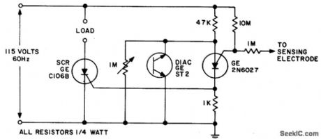
This circuit is actuated by an increase in capacitance between a sensing electrode and the ground side of the line. The sensitivity can be adjusted to switch when a human body is within inches of the insulated plate used as the sensing electrode. Thus, sensitivity is adjusted with the 1 megohm potentiometer which de-termines the anode voltage level prior to clamping. This sensitivity will be proportional to the area of the surface opposing each other. (View)
View full Circuit Diagram | Comments | Reading(1389)
PHOTO_STROBE
Published:2009/6/24 23:00:00 Author:Jessie

Sound or light sensors connected to J2 produce a voltage that is amplified by IC1-a and IC1-b. A positive trigger voltage that is developed by D1 and D3 and amplified by IC1-d, drives IC2 and IC1 to trigger SCR1. SCR1 is connected to a strobe. This device is handy for photographic purposes to take pictures of events that involve sound, such as impacts, etc. (View)
View full Circuit Diagram | Comments | Reading(1426)
VIDEO_TITLER
Published:2009/6/24 21:38:00 Author:May

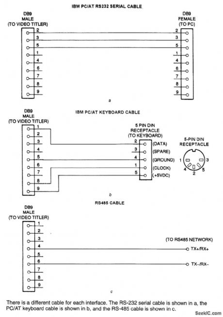
The figure shows the schematic of the video titler circuit. The power-on reset function is generated by IC7, a Maxim MAX699 reset, and watchdog pulse generator. That device supplies a reset pulse of 140 to 500 ms at power-up. This is accomplished with some external parts, as well as the OSD controller in IC1. First, the horizontal and vertical sync from the composite video input is detected by IC2, which is set for NTSC specification horizontal and vertical synchronization timing via resistor R4.The detected horizontal and vertical sync is fed to IC1. The OSC controller in IC1 uses these sig-nals to internally synchronize the overlay text to the incoming video. The frequency of the dot clock is controlled by components L1, C5, and C6. Text is overlaid by video multiplexer IC5, which is con-trolled by IC1.The overlay character outline and intensity are controlled via solid-state potentiometers, allow-ing the microcontroller to control the position of their wipers and store the settings in an onboard EEPROM. The microcontroller's OSC logic controls the multiplexer timing from the BF (IC1, pin 30) and VIDCTL (IC1, pin 25) signals. The BF signal switches the video multiplexer between character and character-outline video, and VIDCTL switches the multiplexer between the input video and the overlay video from IC1. The dc levels from IC3 and IC4 set the character and outline intensity, and these levels are fed to video multiplexer IC5.The video titler can store and recall text from EEPROM IC6, which has enough capacity to store one overlay screen and other required data, such as network address, horizontal and vertical overlay fine position, and type of interface.The RS-232 interface is provided by a MAX202 transceiver. The RS-485 interface is provided by an LTC485 transceiver that provides both transmit and receive functions. The keyboard interface is basically a direct connection to the microprocessor. (View)
View full Circuit Diagram | Comments | Reading(859)
SIMPLE_NTSC_GRAY_SCALE_VIDEO_GENERATOR
Published:2009/6/24 21:46:00 Author:Jessie

A 4.032-MHz crystal oscillator (256 x horizontal line scan rate) drives a BCD counter. The binary outputs of the counter are fed to R2 through R5, a simple weighting network for D/A conversion, re-sulting in a staircase video output with a rep rate of 15.75 kHz. This circuit should be useful for am-ateur TV linearity testing and setup purposes. (View)
View full Circuit Diagram | Comments | Reading(0)
| Pages:78/126 At 206162636465666768697071727374757677787980Under 20 |
Circuit Categories
power supply circuit
Amplifier Circuit
Basic Circuit
LED and Light Circuit
Sensor Circuit
Signal Processing
Electrical Equipment Circuit
Control Circuit
Remote Control Circuit
A/D-D/A Converter Circuit
Audio Circuit
Measuring and Test Circuit
Communication Circuit
Computer-Related Circuit
555 Circuit
Automotive Circuit
Repairing Circuit